P-N Junction Biasing and Characteristics
Step by step video solution for P-N Junction Biasing and Characteristics by Physics experts to help you in doubts & scoring excellent marks in Class 11 exams.
Updated on:21/07/2023Similar Questions
Knowledge Check
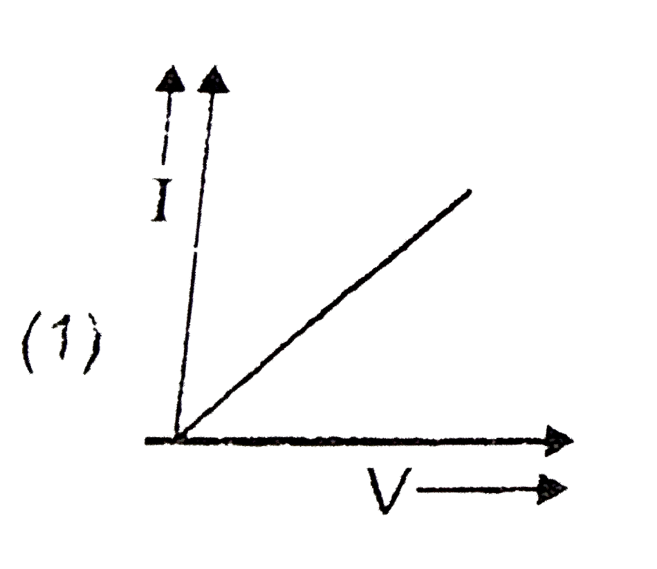
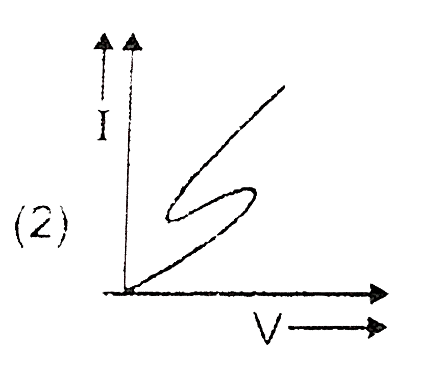
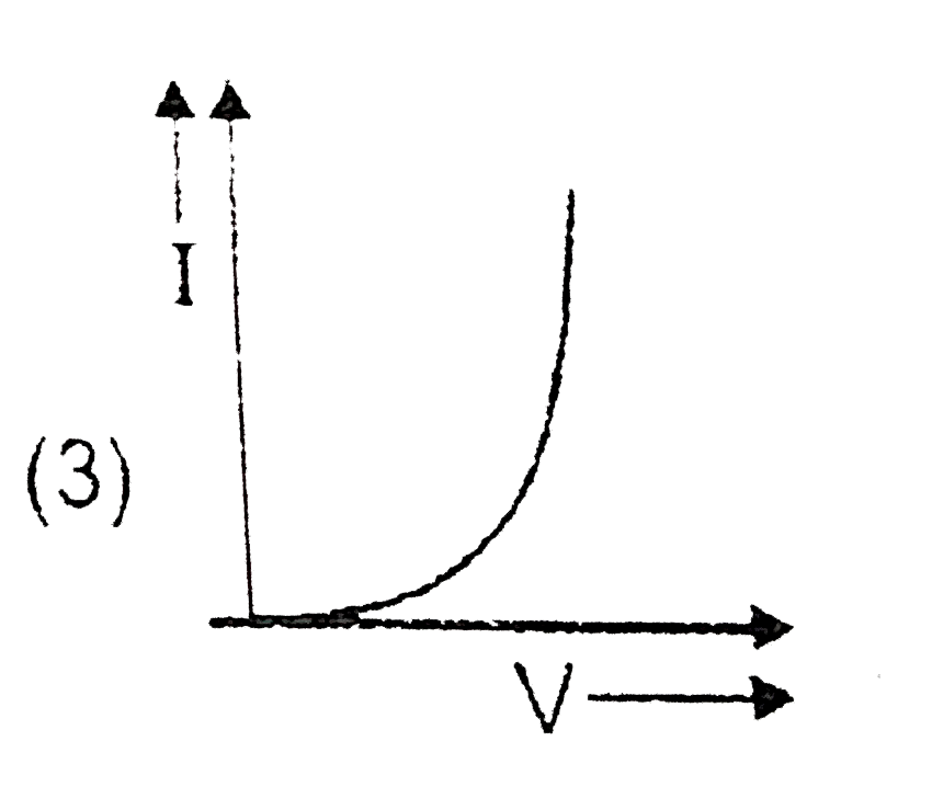
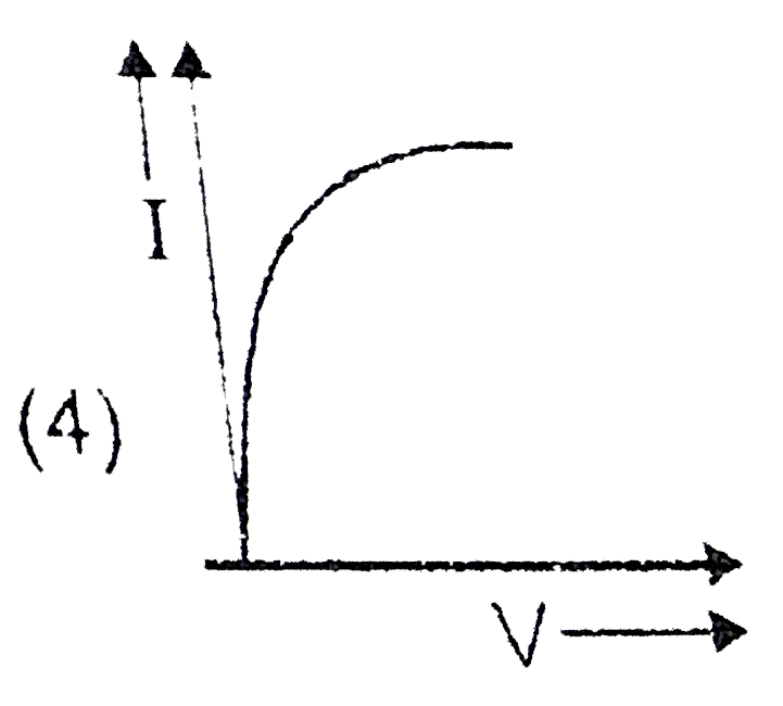
Choose the correct option for the forward biased characteristics of a p-n junction
A B
B C
C D
D
In V- I characteristics of p−n junction in reverse biasing results in
Aleakeage currentBthe current which cannot be neglectedCno flow of currentDlarge currentp-n junction is called as forward biased when
Apositive terminal of the battery is connected to the p-type semiconductor and negative is connected to the n-type semiconductorBpositive terminal of battery is connected to the n-type semiconductor and negative terminal is connected to the p-type semiconductorCpositive terminal of battery is connected to the n-type of semiconductorDa mechanical force is applied in forward direction
Using the necessary circuit diagram, show how the V-I characteristics of a p-n junction are obtained in (i) forward biasing (ii) Reverse biasing. How are these characteristics made use of in rectification?
View SolutionUsing the necessary circuit diagram, show how the V-I characteristics of a p-n junction are obtained in (i) forward biasing (ii) Reverse biasing. How are these characteristics made use of in rectification?
View SolutionP-N Junction Formation||Junction Voltage and depletion Layer||Biasing OF a P-N junction||Forward and Reverse Biasing||V-I Characterstic OF a P-N Junction||Resistance OF a P-N Junction||Dynamic Resistance OF a P-N junction|| Characterstics OF an ideal diode
View SolutionP-N Junction|P-N Junction Diode Under Forward Bias
View SolutionOn adjusting the P−N junction diode in forward biased
View Solution
