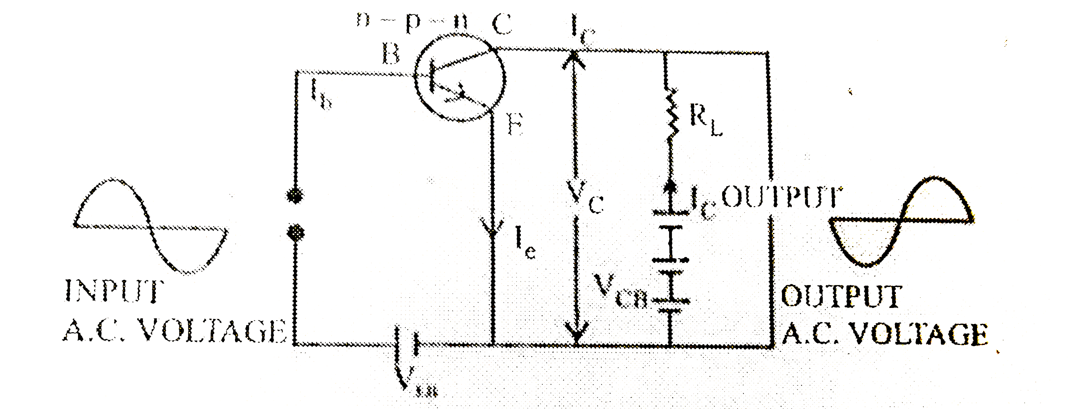
Draw the labelled circuit diagram of a common-emitter transistor amplifie : Explain clearly how the input and output signals are in opposite phase.
The circuit details for using an npn transistor as common emitter amplifier are shown in the fig.

The input (base-emitter) circuit is forward biased and the output (collector-emitter) circuit is reverse biased.
When no a.c. signal is applied, the potential difference Vc between the collector and the emitter , is given by
VC=VCE−IC×RL ...(i)
Where, VC is the voltage of battery VCE
When an a.c. signal is fed to the input circuit, the forward bias increases during the positive half cycle of the input. This results in an increase in IC and a consequent decrease in VC, as is clear from (i). Thus during positive half cycle of the input, the collector becomes less positive.
During the negative half cycle of the input, the forward bias is decreased resulting in a decrease in IE and hence IC. Therefore, from (i) VC would increase, making the collector more positive. Hence, in a common-emitter amplifier, the output voltage is 180∘ out of phase with the input voltage.
Topper's Solved these Questions
Similar Questions
Draw the labelled circuit diagram of a common-emitter transistor amplifier : Explain clearly how the input and output signals are in opposite phase.
View SolutionDraw the circuit diagram of a common emitter transistor amplifier. Write the expression for its voltage gain. Explain , how the input and output signal differ in phase by 180∘
View SolutionDraw the circuit diagram of a common emitter transistor amplifier. Write the expression for its voltage gain. Explain , how the input and output signal differ in phase by 180∘
View SolutionDraw a labelled circuit diagram of a transistor acting as a common emitter amplifier. What is meant by phase reversal?
View SolutionGive a circuit diagram of a common emitter amplifier using an n-p-n transistor. Draw the input and output wavefroms of the signal. Write the expression for its voltage gain.
View SolutionDraw the circuit diagram of a common emitter amplifier using n-p-n transistor. What is the phase difference between the input signal and output voltage? State two reasons why a common emitter amplifier is preferred to a common base amplifier.
View SolutionDraw a labelled circuit diagram of a transistor as a switch and draw its input and output graphs.
View SolutionDraw a labelled circuit diagram for a common emitter amplifier using n-p-n transistor. Write down the expression for its voltage gain. What is the phase difference between input and output signals?
View SolutionDraw a labelled circuit diagram of n - p - n germanium transistor in common emitter configuration. Explain briefly, how this transistor is used as a voltage amplifier.
View SolutionIn common emitter transistor amplifier circuit, the input signal voltage and the output collector voltage are ..............phase.
View Solution

