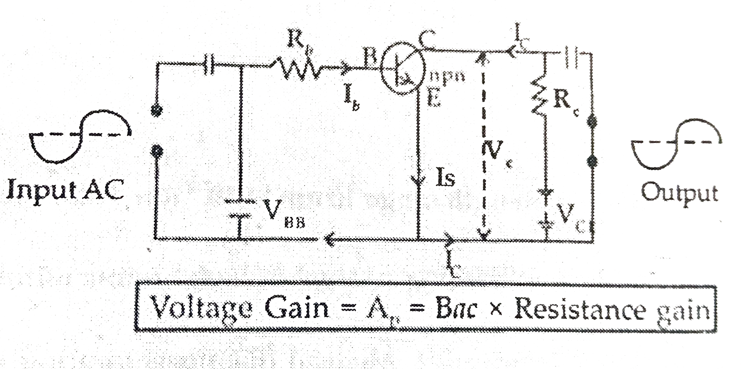
Draw the circuit diagram of a common emitter transistor amplifier. Write the expression for its voltage gain. Explain , how the input and output signal differ in phase by 180∘

During positive half cycle of input single, forward bias of EB junction decreases casuing. Ie and hence Ic decreases. It results in voltage drop across load resistance RL. So, from the relation.
VCE=VCC−ICRL,V0 increases.
As collector is connected to the negative terminal of battery, increase in collector voltage indicates that collector becomes more negative. As in common ammeter amplifier, the output voltage decreases with increases in input signal and increases with decreasing input signal, so both input and output signals are out of phase with phase difference π. During negative half cycle of input signal, the forward bias of EB junction decreases. As a result, IE and hence IC decreases. Voltage Drop across RL=ICRL also decreases. So, the output voltage increases. As collector is connected to the positive terminal of VCC, so, increase in V0⇒ collector voltage will be more positive. An amplified positive signal is obtained across the output.
Topper's Solved these Questions
- BOOK - XII BOARD PREVIOUS YEAR PAPER ENGLISHCHAPTER - XII BOARDSEXERCISE - PHYSICS (Theory) DELHI BOARD -2016 [SET -I][COMPTT.]11videos
XII BOARDS
- BOOK - XII BOARD PREVIOUS YEAR PAPER ENGLISHCHAPTER - XII BOARDSEXERCISE - C.B.S.E.CLASS-XII PHYSICS (THEORY) [SET-I] (SECTION-A)5videos
XII BOARDS
- BOOK - XII BOARD PREVIOUS YEAR PAPER ENGLISHCHAPTER - XII BOARDSEXERCISE - SECTION-B52videos
XII BOARDS
- BOOK - XII BOARD PREVIOUS YEAR PAPER ENGLISHCHAPTER - SAMPLE PAPER 2019EXERCISE - SECTION D6videos
SAMPLE PAPER 2019
Similar Questions
Knowledge Check
- Question 1 - Select One
The input resistance of a common emitter transistor amplifier, if the output resistance is 500kΩ, the current gain α=0.98 and the power gain is 6.0625×10⁶ is
A198ΩB300ΩC100ΩD400Ω
Draw a circuit diagram of C.E. transistor amplifier. Briefly explain its working and write the expression for (i) current gain (ii) voltage gain of the amplifier.
View SolutionThe frequency of oscillation of current in the indcutor is
 View Solution
Give a circuit diagram of a common emitter amplifier using an n-p-n transistor. Draw the input and output wavefroms of the signal. Write the expression for its voltage gain.
View SolutionIn a common emitter amplifier, the input and output voltage are out of phase by
View SolutionDraw a labelled circuit diagram of a transistor acting as a common emitter amplifier. What is meant by phase reversal?
View SolutionIn a common emitter amplifier circuit using an n-p-n transistor, the phase difference between the input and the output voltages will be:-
View SolutionDraw a labelled circuit diagram of n - p - n germanium transistor in common emitter configuration. Explain briefly, how this transistor is used as a voltage amplifier.
View Solution

