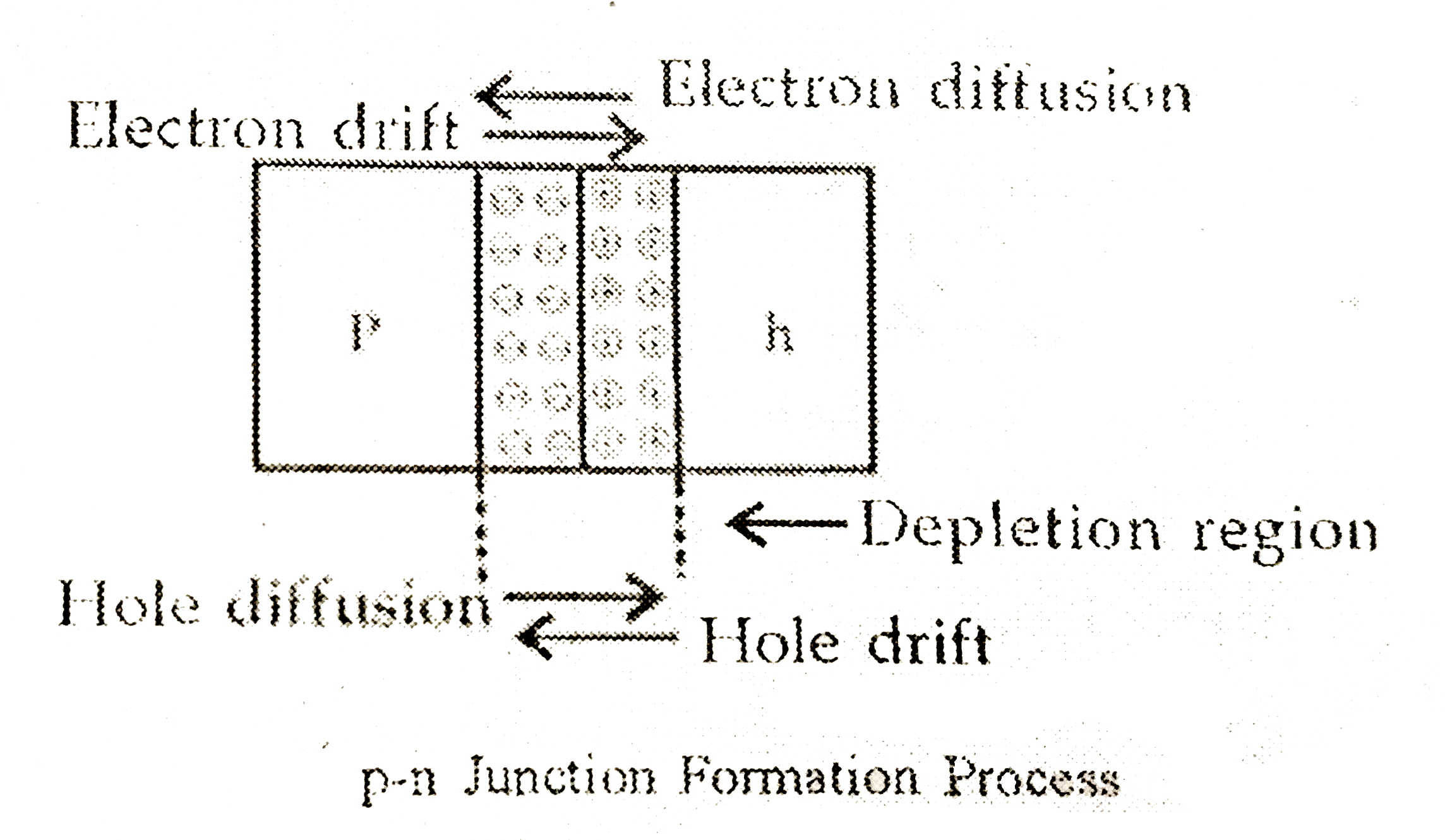
(a) Explain with the help of suitable diagram , the two processes which occur during the formations of a p -n junction diode . Hence , define the terms :
(i) depletion region and (ii) potential barrier :
(b) Draw a circuit diagram of a p - n junction diode under forward bias and explain its working .
Text Solution
(a) (i) Depletion region : Two important processes occur during the formation of - p - n junction : diffusion and drift . In n type semiconductor , the concentration of electron is more compared to the concentration of holes is more than the concentration of electrons . During the formation of p - n junction , and due to the concentration gradient across p - and n - sides holes diffuse from p side to n side and electron diffuse from n - side to p - side .
When an electron diffuses from n→p , it leaves behind an ionised donor on n side . This ionised doner is immobile as it is bonded to the surrounding atom .
When the hole diffuses from p→n due to concentration gradiant , it leaves behind an ionised acceptor negative ion . This space charge region on either side of the junction together is known as depletion region.
(ii) Barrier potential : When there is a diffusion of holes from p region to n region and diffusion of electrons in the reverse direction takes place , part of depletion layer on n side of junction becomes positively charged and the part of depletion layer on p side of the junction becomes negatively charged. Due to this , a junction potential is developed , which opposes further diffusion of holes and electrons . Hence , this potential acts as a barrier and is known as ' barrier potential'.

|
Topper's Solved these Questions
- XII BOARDSBOOK - XII BOARDS PREVIOUS YEARCHAPTER - XII BOARDSEXERCISE - SECTION - C
13 Videos
- XII BOARDSBOOK - XII BOARDS PREVIOUS YEARCHAPTER - XII BOARDSEXERCISE - SECTION - A
7 Videos
- XII BOARDSBOOK - XII BOARDS PREVIOUS YEARCHAPTER - XII BOARDSEXERCISE - SECTION - D
6 Videos
- SAMPLE PAPER 2019BOOK - XII BOARDS PREVIOUS YEARCHAPTER - SAMPLE PAPER 2019EXERCISE - SECTION D
6 Videos
Similar Questions
Knowledge Check
With forward biased mode, the p-n junction diode
Ain one is which width of depletion layer increasesBis one in which potential barier increasesCacts as closed switchDacts as open switchWith in depletion region of p-n junction diode :
Ap-side is positive and n-side is negativeBn-side is positive and p-side is negativeCboth side are positive and both side are negativeDboth side are neutralWith in depletion region of p-n junction diode :
Ap-side is positive and n-side is negativeBn-side is positive and p-side is negativeCboth side are positive and both side are negativeDboth side are neutral
Explain the formation of depletion layer and potential barrier in p-n junction.
Draw the circuit diagram of a half wave rectifier and explain its working.
View SolutionExplain the formation of depletion layer and potential barrier in p-n junction.
Draw the circuit diagram of a half wave rectifier and explain its working.
View SolutionP-N Junction|P-N Junction Diode Under Forward Bias
View SolutionExplain the term depletion region and potential barrier for a p-n junction.
View SolutionIn the forward bias arrangement of a p-n junction diode
View Solution
