(a) Describe briefly the functions of the three segments of n-p-n transistor.
(b) Draw the circuit arrangment for studying the output characterstics of n-p-n transistor in CE configuration. Explain how the output characterstics is obtained.
(a) A junction transistor is obtained by growing a thin layer of one type semi-conductor in between two thick layers of other similar type semi-conductors.
Three layers and functions
Emitter ( E) : The left hand thick layer of the transistor which is heavily doped and moderate in size is called emitter. If emits majority charge carriers.

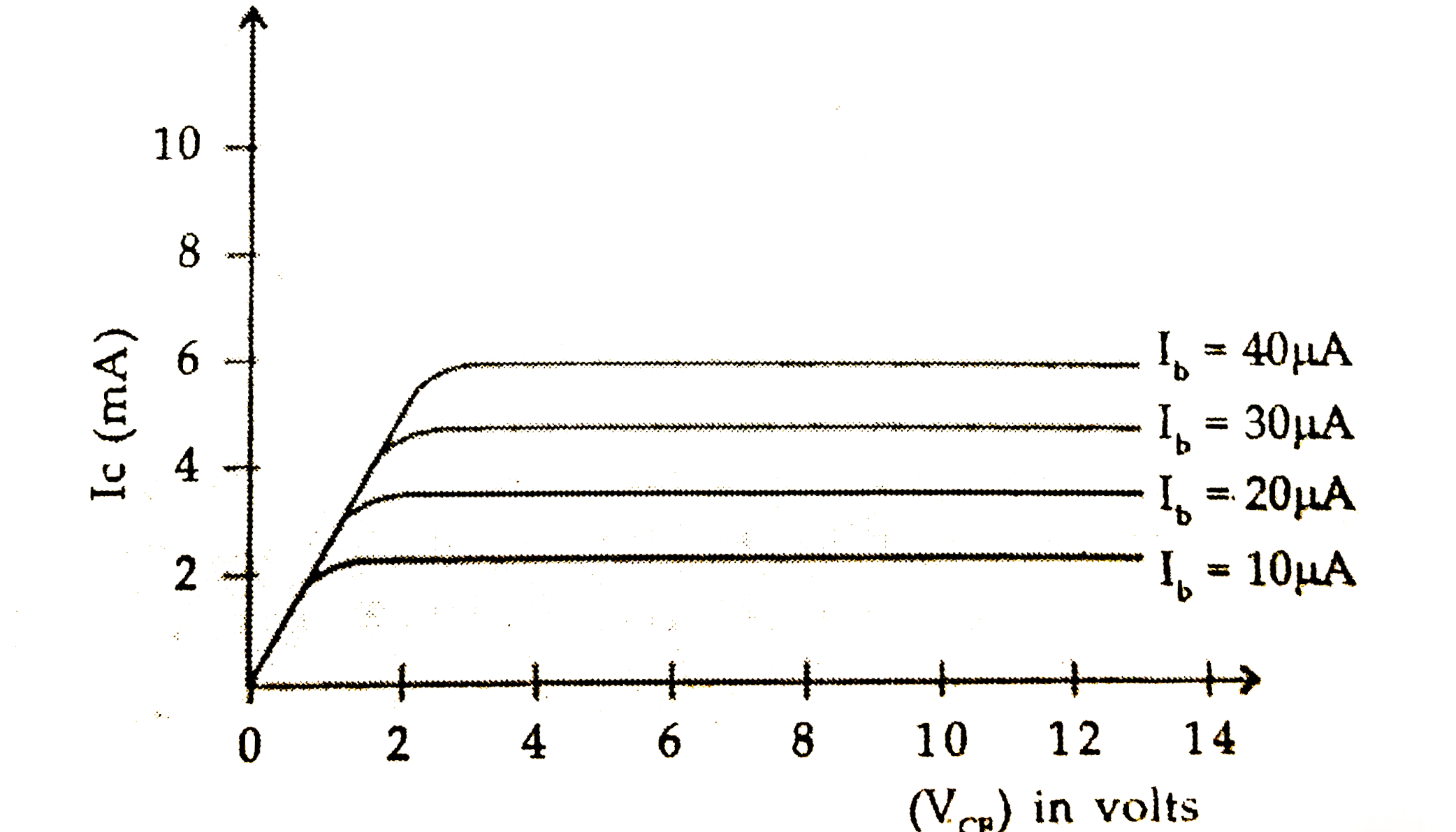
Output Characteristics : The variation fo the collector. Current (Ic) with the collector emitter voltage (VCE) keeping the base current (Ib) constant is called output characteristics.
(i) Baxe (B) : It is a central thick layer of the transistor which is lightly deped. Correlates interaction between emitter and collector.
(iii) Collector ( C) : The right hand hand side thick layer of the transistor which is moderately deped is called collector. It collect the majority charge carriers.

Topper's Solved these Questions
- XII BOARDSBOOK - XII BOARDS PREVIOUS YEARCHAPTER - XII BOARDSEXERCISE - PHYSICS (Theory) DELHI BOARD -2016 [SET -I][COMPTT.]
12 Videos
- XII BOARDSBOOK - XII BOARDS PREVIOUS YEARCHAPTER - XII BOARDSEXERCISE - C.B.S.E.CLASS-XII PHYSICS (THEORY) [SET-I] (SECTION-A)
5 Videos
- XII BOARDSBOOK - XII BOARDS PREVIOUS YEARCHAPTER - XII BOARDSEXERCISE - SECTION-B
65 Videos
- SAMPLE PAPER 2019BOOK - XII BOARDS PREVIOUS YEARCHAPTER - SAMPLE PAPER 2019EXERCISE - SECTION D
6 Videos
Similar Questions
(i) Write the functions of three segments of a transistor.
(ii) Draw the ciruit diagram or studying the input and output characteristics of n-p-n transisfor in common emitter configuration . Using the circuit explain how input characteristics are obtained .
View SolutionDraw a circuit diagram to obtain the characteristics of a n-p-n transistor in common base configuration . Give shape of input and output characteristic curves.
View Solution
Knowledge Check

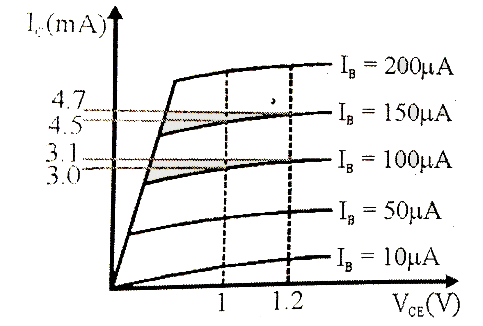
Output characteristic of n-p-n transistor in CE configuration is shown. From the characteristic curve determine the current gain at VCE=1V-A30B32C28D40In an n-p-n transistor in CE configuration when VBE is increased by small amount, then
AIB increases and IC increases proportionatelyBIB increases and IC remains constantCIB remains constant and IC increasesDBoth IB and IC remain nearly constant
Draw the circuit diagram for studying the characteristics of a transistor in common emitter configuration. Explain briefly and show how input and output characteristics are drawn.
View SolutionDraw the diagram of the circuit arangement used for studying the 'input' and the 'output' characteristics of an n-p-n transistor inits CE configuration. Briefly explain how these two types of characteristics are obtained and draw these characteristics.
(b) 'Define' the terms (i) Input resistance, (ii) Output resistance , (iii) Current amplification factor, for a given transistor.
View SolutionDraw typical output characteristics of an n-p-n transistor in CE configuration. Show how these characteristics can be used to determine output resistance.
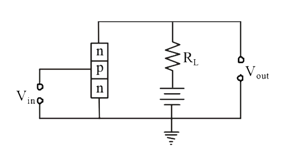
View SolutionAn n-p-n transistor circuit is arranged as shown in fig. It is -

View SolutionSketch the three modes of study of n-p-n junction transistor.
View Solution(a) Draw the circuit arrangement for studying the input and output characteristics of an n-p-n transistor in CE configuration . With the help of these characteristics define (i) input resistance , (ii) current amplification factor .
(b) Describe briefly with the help of a circuit diagram how an n-p-n transistor is used to produce self-sustained oscillations .
View Solution
