What is depletion barrier? Solution in Gujrati
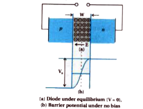
Due to diffusion of charge carriers in p-n junction, the number of electron decreases in the n-section and the number of electron in p-section increases so that potential difference across junction is developed.
The polarity of this potential is such as to oppose further flow of carriers so that a condition of equilibrium exists.

Figure shows the p-n junction at equilibrium and the potential across the junction.
The n-material has lost electrons and p-materials has acquired electrons.
This potential tends to prevent the movement of electron from the n-region into p-region it is called a barrier potential. This barrier is obtained in the depletion region, hence it is also called depletion barrier.
Topper's Solved these Questions
- BOOK - KUMAR PRAKASHANCHAPTER - SEMICONDUCTOR ELECTRONICS : MATERIALS, DEVICES AND SIMPLE CIRCUITS EXERCISE - Section-B : Numericals (Numerical From Textual illustrations)16videos
SEMICONDUCTOR ELECTRONICS : MATERIALS, DEVICES AND SIMPLE CIRCUITS
- BOOK - KUMAR PRAKASHANCHAPTER - SEMICONDUCTOR ELECTRONICS : MATERIALS, DEVICES AND SIMPLE CIRCUITS EXERCISE - Section-B : Numericals (Numerical From Textual Exercise)15videos
SEMICONDUCTOR ELECTRONICS : MATERIALS, DEVICES AND SIMPLE CIRCUITS
- BOOK - KUMAR PRAKASHANCHAPTER - SEMICONDUCTOR ELECTRONICS : MATERIALS, DEVICES AND SIMPLE CIRCUITS EXERCISE - Section-D : Multiple Choice Questions (MCQs) (MCQs asked in Competitive Exams)129videos
SEMICONDUCTOR ELECTRONICS : MATERIALS, DEVICES AND SIMPLE CIRCUITS
- BOOK - KUMAR PRAKASHANCHAPTER - SAMPLE QUESTION PAPER EXERCISE - PART-B SECTION-C5videos
SAMPLE QUESTION PAPER
- BOOK - KUMAR PRAKASHANCHAPTER - WAVE OPTICSEXERCISE - SECTION-D (MULTIPLCE CHOICE QUESTIONS (MCQS)) (MCQS FROM DARPAN BASED ON TEXTBOOK)239videos
WAVE OPTICS
Similar Questions
C, Si and Ge have same lattice structure. Why is C insulator while Si and Ge intrinsic semiconductors?
03:49View SolutionIn an n type silicon, which of the following statements is true:
02:05View SolutionAt absolute zero temperature Si acts as ……..
03:03View SolutionTwo charges –q and +q are located at points (0, 0, –a) and (0, 0, a), respectively.
(a) What is the electrostatic potential at the points (0, 0, z) and (x, y, 0) ?
(b) Obtain the dependence of potential on the distance r of a point from the origin when r/a>>1 .
(c) How much work is done in moving a small test charge from the point (5,0,0) to (–7,0,0) along the x-axis? Does the answer change if the path of the test charge between the same points is not along the x-axis?02:54View SolutionAccording to particle theory of light what is the velocity of light in a dense medium, compared to that in rare medium ?
02:31View SolutionDepletion Region And Barrier Electric Field
02:23View SolutionIn a forward biased PN- junction diode, the potential barrier in the depletion region is of the from...
05:03View SolutionExplain the term depletion region and potential barrier for a p-n junction.
03:19View SolutionThe potential barrier in the depletion layer is due to
06:55View SolutionThe potential barrier, in the depletion layer, is due to
01:19View SolutionThe potential barrier in the depletion layer is due to
02:00View SolutionQ6.When "p" - "n" junction diode is forward biased,then (a)the depletion region is reduced and barrier height is increased (b) the depletion region is widened and barrier height is reduced (c)both the depletion region and barrier height are reduced (d) both the depletion region and barrier height are increased
08:12View SolutionIn a forward biased p-njunction diode, the potential barrier in the depletion region is of the form
05:35View SolutionWhat is depletion barrier?
09:22View SolutionIn p-n junction, depletion barrier near the junction is due to ………
04:24View SolutionWhat is responsible for depletion barrier in depletion layer?
01:03View Solution

