Write the symbol, truth table, function and Boolean equation for AND gate. Solution in Gujrati
Figure (a) shown the symbolic figure of ANI gate. This gate has two or more inputs and one output.

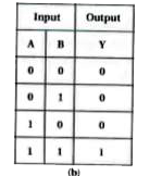
Function : The output Y and AND gate is only when input A and input B are both 1. We get the output O for all remaining values.
Boolean equation of AND gate is Y = A • B. Here .•. is known as AND operator. The equation is read as "Y is equal to A AND B".
Truth table for AND gate is shown in figure (b).

This gate is also used for performing mathematical function as well as for modifying the pulse waveform.
Topper's Solved these Questions
- BOOK - KUMAR PRAKASHANCHAPTER - SEMICONDUCTOR ELECTRONICS : MATERIALS, DEVICES AND SIMPLE CIRCUITS EXERCISE - Section-B : Numericals (Numerical From Textual illustrations)16videos
SEMICONDUCTOR ELECTRONICS : MATERIALS, DEVICES AND SIMPLE CIRCUITS
- BOOK - KUMAR PRAKASHANCHAPTER - SEMICONDUCTOR ELECTRONICS : MATERIALS, DEVICES AND SIMPLE CIRCUITS EXERCISE - Section-B : Numericals (Numerical From Textual Exercise)15videos
SEMICONDUCTOR ELECTRONICS : MATERIALS, DEVICES AND SIMPLE CIRCUITS
- BOOK - KUMAR PRAKASHANCHAPTER - SEMICONDUCTOR ELECTRONICS : MATERIALS, DEVICES AND SIMPLE CIRCUITS EXERCISE - Section-D : Multiple Choice Questions (MCQs) (MCQs asked in Competitive Exams)129videos
SEMICONDUCTOR ELECTRONICS : MATERIALS, DEVICES AND SIMPLE CIRCUITS
- BOOK - KUMAR PRAKASHANCHAPTER - SAMPLE QUESTION PAPER EXERCISE - PART-B SECTION-C5videos
SAMPLE QUESTION PAPER
- BOOK - KUMAR PRAKASHANCHAPTER - WAVE OPTICSEXERCISE - SECTION-D (MULTIPLCE CHOICE QUESTIONS (MCQS)) (MCQS FROM DARPAN BASED ON TEXTBOOK)239videos
WAVE OPTICS
Similar Questions
C, Si and Ge have same lattice structure. Why is C insulator while Si and Ge intrinsic semiconductors?
02:21View SolutionIn an n type silicon, which of the following statements is true:
02:19View SolutionAt absolute zero temperature Si acts as ……..
03:18View SolutionTwo charges –q and +q are located at points (0, 0, –a) and (0, 0, a), respectively.
(a) What is the electrostatic potential at the points (0, 0, z) and (x, y, 0) ?
(b) Obtain the dependence of potential on the distance r of a point from the origin when r/a>>1 .
(c) How much work is done in moving a small test charge from the point (5,0,0) to (–7,0,0) along the x-axis? Does the answer change if the path of the test charge between the same points is not along the x-axis?05:22View SolutionAccording to particle theory of light what is the velocity of light in a dense medium, compared to that in rare medium ?
05:05View SolutionOR गेट के लिए सत्यता सारणी लॉजिक प्रतीक , बूलियन व्यंजक तथा सत्यता सारणी दीजिए ।
03:51View SolutionOR गेट के लिए सत्यता सारणी लॉजिक प्रतीक , बूलियन व्यंजक तथा सत्यता सारणी दीजिए ।
01:06View SolutionNAND गेट की सत्यता सारणी तथा बुलियन व्यंजक लिखें।
01:24View SolutionWrite logic symbol boolean expression and truth table of AND andNOR gate
01:16View SolutionWrite logic symbol boolean expression and truth table of NAND and OR gate
01:25View SolutionWrite logic symbol boolean expression and truth table of NOT and OR gate ]
02:09View SolutionWrite the symbol, truth table, function and Boolean equation for NOT gate.
03:27View SolutionWrite the symbol, truth table, function and Boolean equation for OR gate.
03:24View SolutionWhat is NAND gate? Write its symbol, truth table and Boolean equation.
03:00View SolutionWhat is NOR gate? Write its symbol, truth table and Boolean equation.
03:29View Solution

