Suppose a 'n'-type wafer is created by dopin Si crystal having 5×1028 atoms/m3 with 1 ppm concentration of As. On the surface 200 ppm Boron is added to create 'P' region in this wafer. Considering ni=1.5×10¹⁶m−3 (i) Calculate the denisties of the charge carrier in the n & p regions. (ii) Comment which charge carriers would contribute largely for the reverse saturation current when diode is reverse biased. Solution in Gujrati
Here 1 ppm = 1 part per million
= 1 part in 10 lakh
(i) For n-type semiconductor :
(no. of Si atoms in 1 m3 volume) → (no. of As atoms in 1 m3 volume)
106→1
∴5×1028→(?)
⇒ Number density of pentavalent As atoms (or) free electron number density).
ne=5×1028106=5×10²²free electronm3
Now nenh=n2i
∴nh=n2ine
=(1.5×10¹⁶)25×1022
∴nh=4.5×10⁹hole/m3 ...(1)
(ii) For p-type semiconductor:
(no. of Si atoms in 1 m3 volume) → (no. of B atoms in 1 m3 volume)
106→200
∴5×1028→ (?)
⇒ Number density of trivalent B atoms (or hole number density).
nh=200×5×1028106
∴nh=1025holem3
Now nenh=n2i
∴ne=n2inh
∴ne=(1.5×10¹⁶)21×1025
∴ne=2.25×10⁷free electronsm3 ...(2)
Equations (1) and (2) indicate that nh>ne
⇒ In the reverse bias condition of given pn-junction, holes will contribute majority in producing reverse saturation current.
Topper's Solved these Questions
- SEMICONDUCTOR ELECTRONICS : MATERIALS, DEVICES AND SIMPLE CIRCUITS BOOK - KUMAR PRAKASHANCHAPTER - SEMICONDUCTOR ELECTRONICS : MATERIALS, DEVICES AND SIMPLE CIRCUITS EXERCISE - Section-D : Multiple Choice Questions (MCQs) (MCQs From .DARPAN. Based On Textbook)
116 Videos
- SEMICONDUCTOR ELECTRONICS : MATERIALS, DEVICES AND SIMPLE CIRCUITS BOOK - KUMAR PRAKASHANCHAPTER - SEMICONDUCTOR ELECTRONICS : MATERIALS, DEVICES AND SIMPLE CIRCUITS EXERCISE - Section-D : Multiple Choice Questions (MCQs) (MCQs asked in Competitive Exams)
129 Videos
- SEMICONDUCTOR ELECTRONICS : MATERIALS, DEVICES AND SIMPLE CIRCUITS BOOK - KUMAR PRAKASHANCHAPTER - SEMICONDUCTOR ELECTRONICS : MATERIALS, DEVICES AND SIMPLE CIRCUITS EXERCISE - Section-C: NCERT Exemplar Solution (Short Answer Type Questions)
8 Videos
- SAMPLE QUESTION PAPER BOOK - KUMAR PRAKASHANCHAPTER - SAMPLE QUESTION PAPER EXERCISE - PART-B SECTION-C
5 Videos
- WAVE OPTICSBOOK - KUMAR PRAKASHANCHAPTER - WAVE OPTICSEXERCISE - SECTION-D (MULTIPLCE CHOICE QUESTIONS (MCQS)) (MCQS FROM DARPAN BASED ON TEXTBOOK)
239 Videos
Similar Questions
Which of the following is not a conductor of electricity?
View SolutionAt absolute zero temperature Si acts as ……..
View Solution
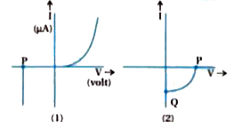
(i) Name the type of a diode whose characteristics are shown in figure (1) and figure (2).
(ii) What does the point P in figure (1) represent?
(iii) What does the points P and Q in figure (2) represent?
View SolutionTwo charges –q and +q are located at points (0, 0, –a) and (0, 0, a), respectively.
(a) What is the electrostatic potential at the points (0, 0, z) and (x, y, 0) ?
(b) Obtain the dependence of potential on the distance r of a point from the origin when r/a>>1 .
(c) How much work is done in moving a small test charge from the point (5,0,0) to (–7,0,0) along the x-axis? Does the answer change if the path of the test charge between the same points is not along the x-axis?
View SolutionAccording to particle theory of light what is the velocity of light in a dense medium, compared to that in rare medium ?
View SolutionSuppose a pure Si-crystal has 5×1028atomsm−3. It is doped by 1 ppm concentration of pentavalent As. Calculate the number of electrons and holes. Give that ni=1.5×10¹⁶m−3.
View SolutionIn the depletion region of an unbiased p-n junction diode, what are the charge carriers?
View SolutionThe number of silicon atoms per m^(3) is 5xx10^(28) . This is doped simultaneously with 5xx10^(22) atoms per m^(3) of Arsenic and 5xx10^(20) per m^(3) atoms of indium. Calculate the number of electrons and holes. Given that n_(i)=1.5xx10^(16)m^(-3) . Is the material n-type or p-type?
View SolutionSuppose a 'n'- type wafer is created by doping Si crystal having 5xx10^(28) "atoms"//m^(3) with 1 ppm concentration of As. On the surfabe 200 ppm Boron is added to create 'p' region in this wafer. Considering n_(i)=1.5xx10^(16)m^(-3) , (i) Calculate the densities of the charge carriers in the n & p regions. (ii) Comment which charge carriers would contribute largely for the reverse saturation current when diode is reverse biased.
View SolutionIn p-n junction, there is a .................of majority carriers across the junction in forward biading and..............of charge carriers in reverse biasing.
View SolutionWhat accounts for the flow of charge carriers in forward and reverse biasing of sillicon P-N diode-
View Solutionमान लीजिए किसी शुद्ध Si क्रिस्टल में 5×1028 परमाणु m−3 है। इसे पंचसंयोजी As से 1ppm सांद्रमा पर अपमिश्रित किया जाता है । इलेक्ट्रॉनों तथा होलों की संख्या परिकलित कीजिए, दिया है कि n1=1.5×10¹⁶m−3
View SolutionP तथा N प्रकार के अर्धचालकों में बहुसंख्यक आवेश वाहक होते है- (i)............., (ii).....................
View SolutionSuppose a pure Si-crystal has 5×1028atomsm−3. It is doped by 1 ppm concentration of pentavalent As. Calculate the number of electrons and holes. Give that ni=1.5×10¹⁶m−3.
View SolutionThe number of silicon atoms per m^(3) is 5xx10^(28) . This is doped simultaneously with 5xx10^(22) atoms per m^(3) of Arsenic and 5xx10^(20) per m^(3) atoms of indium. Calculate the number of electrons and holes. Given that n_(i)=1.5xx10^(16)m^(-3) . Is the material n-type or p-type?
View Solution
