In V-I characteristics of a p-n junction diode, why is the current under reverse bias almost independent of the applied potential upto a critical voltage?
To understand why the current under reverse bias in a p-n junction diode is almost independent of the applied potential up to a critical voltage, we can break down the explanation into clear steps:
1. Understanding Reverse Bias:
- In reverse bias, the p-side (anode) of the diode is connected to the negative terminal of the voltage source, and the n-side (cathode) is connected to the positive terminal. This configuration widens the depletion region.
Hint: Remember that in reverse bias, the direction of the applied voltage opposes the built-in potential of the diode.
2. Depletion Region Expansion:
- When reverse bias is applied, the electric field across the depletion region increases. This causes the majority carriers (holes in the p-region and electrons in the n-region) to be pulled away from the junction, leading to an increase in the width of the depletion region.
Hint: The depletion region is the area where mobile charge carriers are absent, and its width is influenced by the applied voltage.
3. Current Flow in Reverse Bias:
- The current that flows in reverse bias is primarily due to minority charge carriers. In a p-n junction, minority carriers are electrons in the p-region and holes in the n-region. However, this current is very small (typically in the microamp range).
Hint: Focus on the role of minority carriers in the conduction process under reverse bias.
4. Absence of Majority Carrier Flow:
- In reverse bias, there is no diffusion of majority carriers across the depletion region. Since the majority carriers are being pulled away from the junction, they cannot contribute to the current. Therefore, the current is not dependent on the applied reverse voltage.
Hint: Recall that diffusion current requires the movement of majority carriers, which does not occur in reverse bias.
5. Electric Field Contribution:
- The current that does exist is due to the electric field in the depletion region, which can cause minority carriers to drift across the junction. However, this drift current remains constant as the applied reverse voltage increases, up to a certain critical voltage (breakdown voltage).
Hint: The electric field in the depletion region is crucial for understanding how minority carriers contribute to the current.
6. V-I Characteristics:
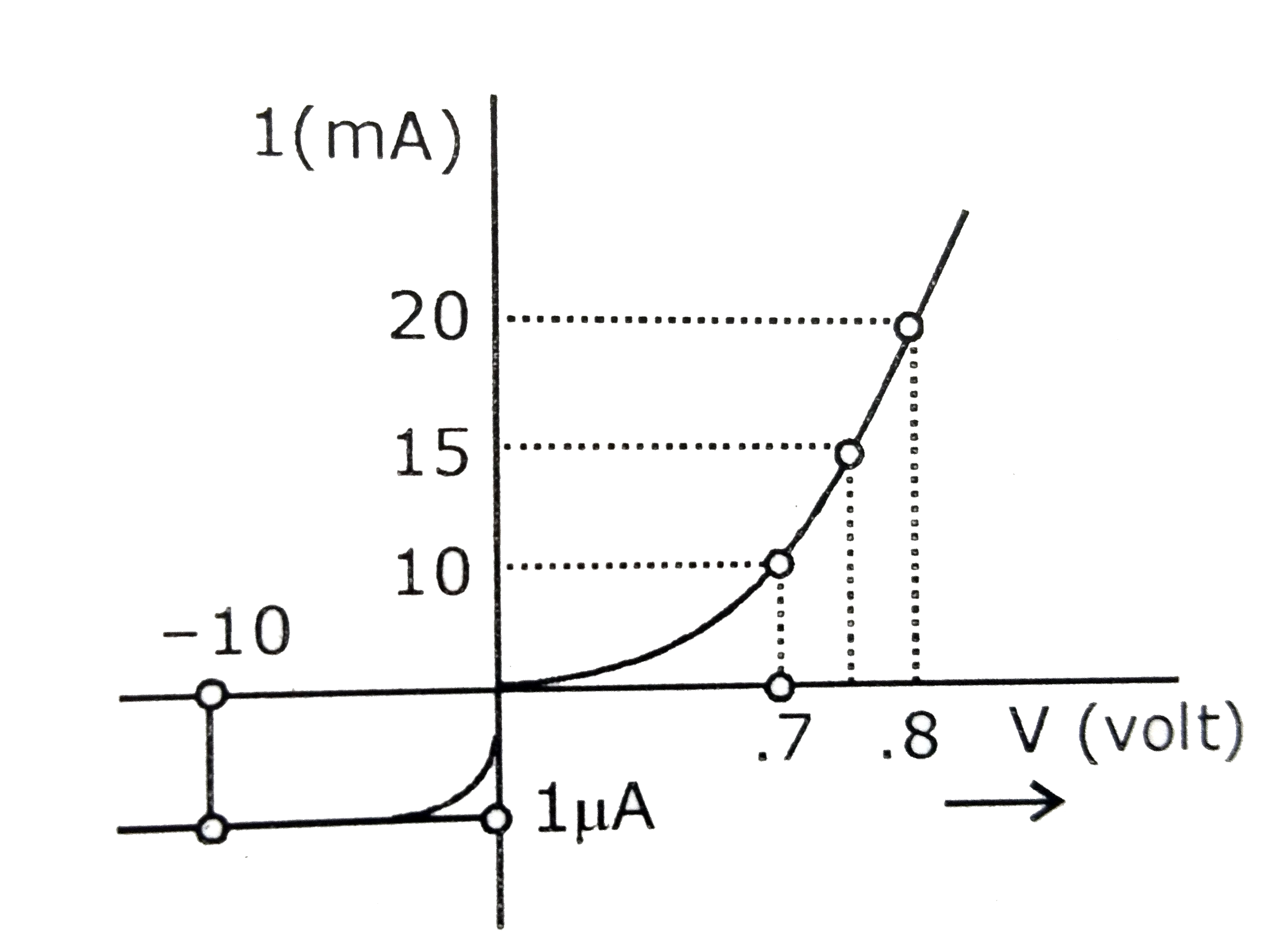
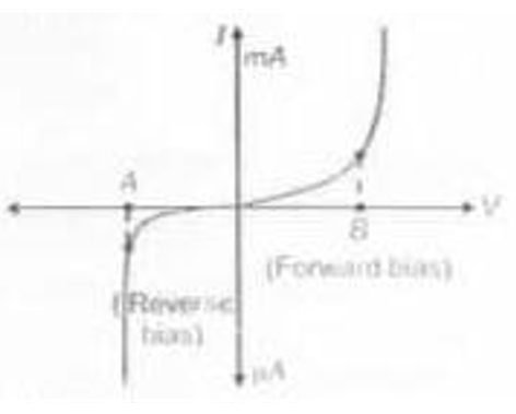
- In the V-I characteristics graph of a p-n junction diode, the reverse current remains almost constant (flat region) until the breakdown voltage is reached. This indicates that the reverse current does not significantly change with increasing reverse voltage.
Hint: Look at the V-I curve to visualize how the current behaves in reverse bias.
Conclusion:
Thus, the current under reverse bias in a p-n junction diode is almost independent of the applied potential up to the critical voltage because the majority carriers do not flow across the depletion region, and the current is primarily due to the minority carriers and the electric field in the depletion region.
- In reverse bias, the p-side (anode) of the diode is connected to the negative terminal of the voltage source, and the n-side (cathode) is connected to the positive terminal. This configuration widens the depletion region.
- When reverse bias is applied, the electric field across the depletion region increases. This causes the majority carriers (holes in the p-region and electrons in the n-region) to be pulled away from the junction, leading to an increase in the width of the depletion region.
- The current that flows in reverse bias is primarily due to minority charge carriers. In a p-n junction, minority carriers are electrons in the p-region and holes in the n-region. However, this current is very small (typically in the microamp range).
- In reverse bias, there is no diffusion of majority carriers across the depletion region. Since the majority carriers are being pulled away from the junction, they cannot contribute to the current. Therefore, the current is not dependent on the applied reverse voltage.
- The current that does exist is due to the electric field in the depletion region, which can cause minority carriers to drift across the junction. However, this drift current remains constant as the applied reverse voltage increases, up to a certain critical voltage (breakdown voltage).
- In the V-I characteristics graph of a p-n junction diode, the reverse current remains almost constant (flat region) until the breakdown voltage is reached. This indicates that the reverse current does not significantly change with increasing reverse voltage.
Thus, the current under reverse bias in a p-n junction diode is almost independent of the applied potential up to the critical voltage because the majority carriers do not flow across the depletion region, and the current is primarily due to the minority carriers and the electric field in the depletion region.
Similar Questions
Draw V-I Characteristics of a p-n junction diode. Answer the following questions, giving reasons-
(i) Why is the current under reverse bias almost independent of the applied potential upto a critical voltage?
(ii) Why does the reverse current show a sudden increase at the critical voltage?
Name any semiconductor device which operates under the reverse bias in the break down region.
View SolutionA p−n junction diode is reverse biased. Then
View Solution
Knowledge Check
In a p−n junction diode, the barrier potential opposes diffusion of
Aminority carrier in both regions onlyBmajority carriers onlyCelectrons in p regionDholes in p region
Barrier potential of a p−n junction diode does not depend on
View SolutionBarrier potential of a p−n junction diode does not depend on
View SolutionForward bias characteristics of a p -n junction diode is used in which of the following devices ?
View SolutionThe V-I characteristic of a diode is shown in the figure. The ratio of forward to reverse bias resistance is

View SolutionThe V-I characteristic of a diode is shown in the figure. The ratio of forward to reverse bias resistance is

View SolutionIn a p-n junction diode the value of drift current through depletion region
View SolutionIn the voltage current (V-l) characteristics of junction diode (figure) the point A and B corresponds to

View Solution
