The ratio (R) of output resistance r0 and the input resistance r, in measurements of input and output charactersitics of a transistor is typically in the range :
R~0.1−1.0
R~102−103
R~0.1−0.01
R~1−10
To solve the problem of finding the ratio R of output resistance r0 to input resistance r in a transistor, we can follow these steps:
1. Understand the Concept:
- The ratio R is defined as:
R=r0r
- Here, r0 is the output resistance and r is the input resistance of the transistor.
2. Identify Typical Values for a BJT:
- For a Bipolar Junction Transistor (BJT), typical values for output resistance r0 can be around 100kΩ.
- The input resistance r can vary, but it is typically in the range of 1kΩ to 10kΩ.
3. Calculate the Minimum Ratio:
- Using the minimum input resistance value:
Rmin=r0rmin=100kΩ1kΩ=100
4. Calculate the Maximum Ratio:
- Using the maximum input resistance value:
Rmax=r0rmax=100kΩ10kΩ=10
5. Express the Ratio in Scientific Notation:
- The minimum ratio Rmin=100 can be expressed as 102.
- The maximum ratio Rmax=10 can be expressed as 103.
6. Final Result:
- Therefore, the ratio R of output resistance to input resistance typically falls within the range:
R≈102 to 103
Conclusion:
The answer is that the ratio R of output resistance r0 to input resistance r in measurements of input and output characteristics of a transistor is typically in the range of 102 to 103.
- The ratio R is defined as:
R=r0r
- Here, r0 is the output resistance and r is the input resistance of the transistor.
- For a Bipolar Junction Transistor (BJT), typical values for output resistance r0 can be around 100kΩ.
- The input resistance r can vary, but it is typically in the range of 1kΩ to 10kΩ.
- Using the minimum input resistance value:
Rmin=r0rmin=100kΩ1kΩ=100
- Using the maximum input resistance value:
Rmax=r0rmax=100kΩ10kΩ=10
- The minimum ratio Rmin=100 can be expressed as 102.
- The maximum ratio Rmax=10 can be expressed as 103.
- Therefore, the ratio R of output resistance to input resistance typically falls within the range:
R≈102 to 103
The answer is that the ratio R of output resistance r0 to input resistance r in measurements of input and output characteristics of a transistor is typically in the range of 102 to 103.
Topper's Solved these Questions
Similar Questions
Input resistance of transistor in comparision to output resistance is-
View Solution(i) Write the functions of three segments of a transistor.
(ii) Draw the ciruit diagram or studying the input and output characteristics of n-p-n transisfor in common emitter configuration . Using the circuit explain how input characteristics are obtained .
View Solution
Knowledge Check
If β,RLandr are the ac current gain, load resistance and the input resistance of a transistor respectively in CE configuration, the voltage and the power gains respectively are
AβRLrandβ2RLrBβrRLandβ2rRLCβRLrandβ(RLr)2DβrRLandβ(rRL)2
Draw the diagram of the circuit arangement used for studying the 'input' and the 'output' characteristics of an n-p-n transistor inits CE configuration. Briefly explain how these two types of characteristics are obtained and draw these characteristics.
(b) 'Define' the terms (i) Input resistance, (ii) Output resistance , (iii) Current amplification factor, for a given transistor.
View SolutionIn a common emitter amplifier, using output reisistance of 5000 ohm and input resistance fo 2000ohm, if the peak value of input signal voltage is 10mV and β=50, then the peak value of output voltage is
View SolutionIn the combination of the following gates the output Y can be written in terms of inputs A and B as

View SolutionPower gain for N−P−N transistor is 10∘, input resistance 100Ω and output resistance 10000Ω. Find out current gain.
View Solution(i) Draw a circuit diagram to study the input and output characteristics of an n-p-n transistor in its common emitter configuration. Draw the typical input and output characteristics.
(ii) Explain, with the hepl of a circuit diagram, the working of n-p-n transistor as a common emitter amplifier.
View Solution(a) Draw the circuit arrangement for studying the input and output characteristics of an n-p-n transistor in CE configuration . With the help of these characteristics define (i) input resistance , (ii) current amplification factor .
(b) Describe briefly with the help of a circuit diagram how an n-p-n transistor is used to produce self-sustained oscillations .
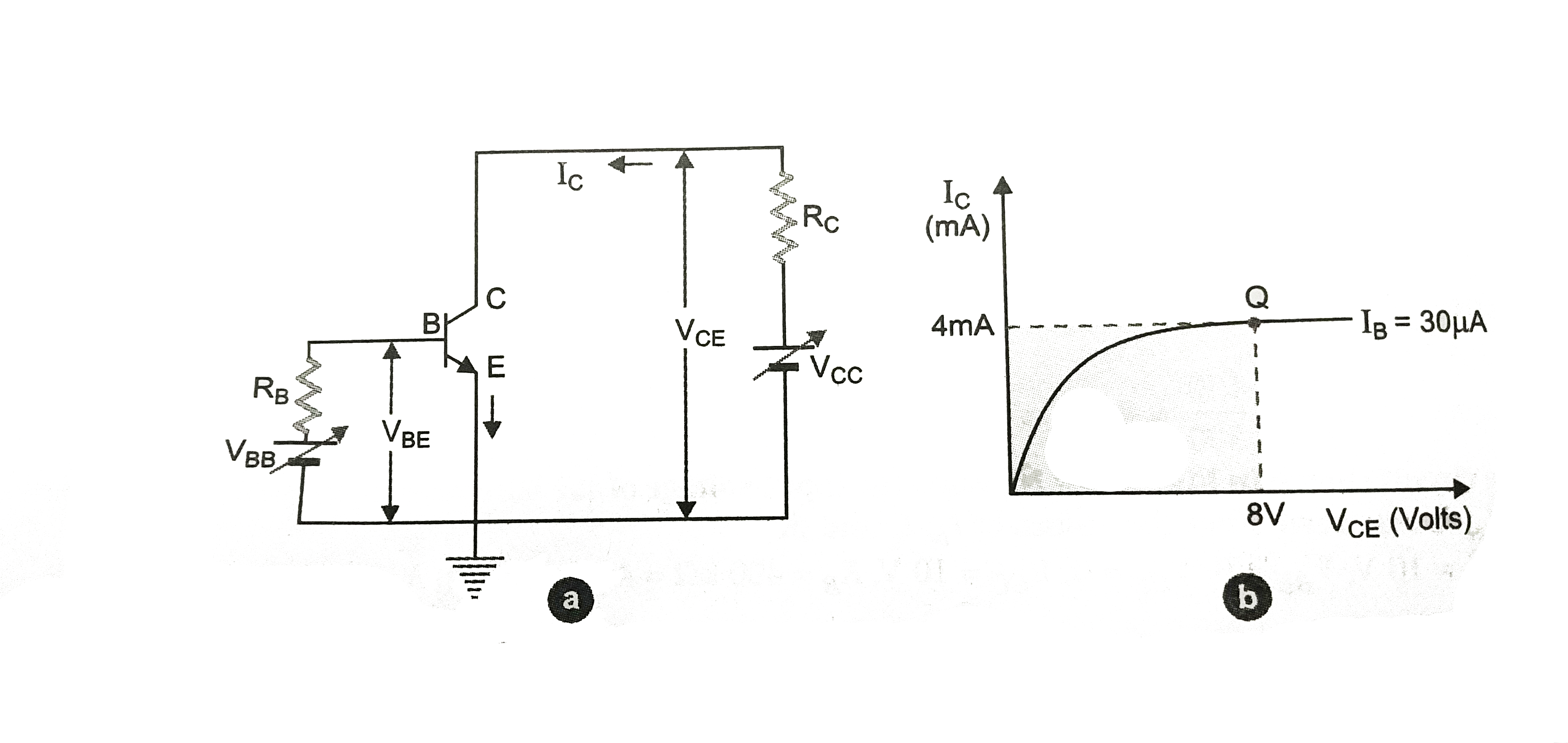
View SolutionConsider the circuit arrangnent shown in Fig. for studying input and output characteristics of npn transistor in CE configuration.
Select the values of R and R for a transistor whose VBE=0.7V, so that the transistor is operating at point Q as shown in the characteristics shown in Fig.
 Given that the input impedance of the transistor is very small and VCC=VBB=16V, also find the voltage gain and power gain of circuit making appropriate assumptions.
View Solution
