Consider the circuit arrangnent shown in Fig. for studying input and output characteristics of npn transistor in CE configuration.
Select the values of and for a transistor whose , so that the transistor is operating at point Q as shown in the characteristics shown in Fig.
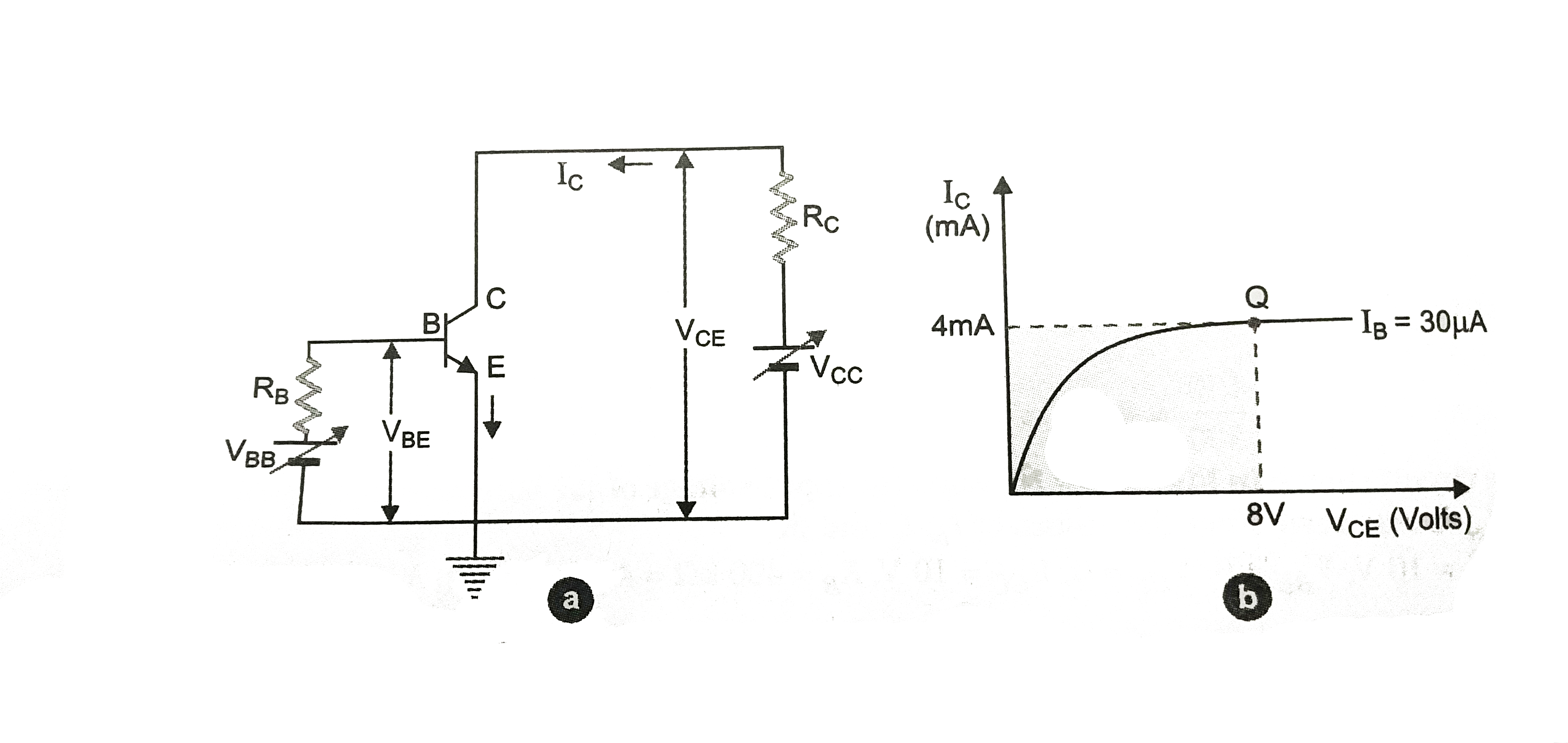 Given that the input impedance of the transistor is very small and , also find the voltage gain and power gain of circuit making appropriate assumptions.
Given,
For the ouput characteristic at ,
Using the relation,
Voltage gain
Power gain Voltage gain
Topper's Solved these Questions
- BOOK - NCERT EXEMPLAR ENGLISHCHAPTER - NUCLEIEXERCISE - Very short Anwer type question14videos
NUCLEI
- BOOK - NCERT EXEMPLAR ENGLISHCHAPTER - MOVING CHARNGES AND MAGNETISMEXERCISE - Long Answer Type Questions7videos
MOVING CHARNGES AND MAGNETISM
- BOOK - NCERT EXEMPLAR ENGLISHCHAPTER - RAY OPTICS AND OPTICAL INSTRUMENTS EXERCISE - VERY SHORT ANSWER TYPE QUESTIONS16videos
RAY OPTICS AND OPTICAL INSTRUMENTS
Similar Questions
Draw typical output characteristics of an n-p-n transistor in CE configuration. Show how these characteristics can be used to determine output resistance.
View Solution(a) Draw the circuit arrangement for studying the input and output characteristics of an n-p-n transistor in CE configuration . With the help of these characteristics define (i) input resistance , (ii) current amplification factor .
(b) Describe briefly with the help of a circuit diagram how an n-p-n transistor is used to produce self-sustained oscillations .View Solution
Knowledge Check
- Question 1 - Select One
In the circuit shown in figure, when the input voltage of the base resistance is 10 V, Vbe is zero and Vce is also zero. Then
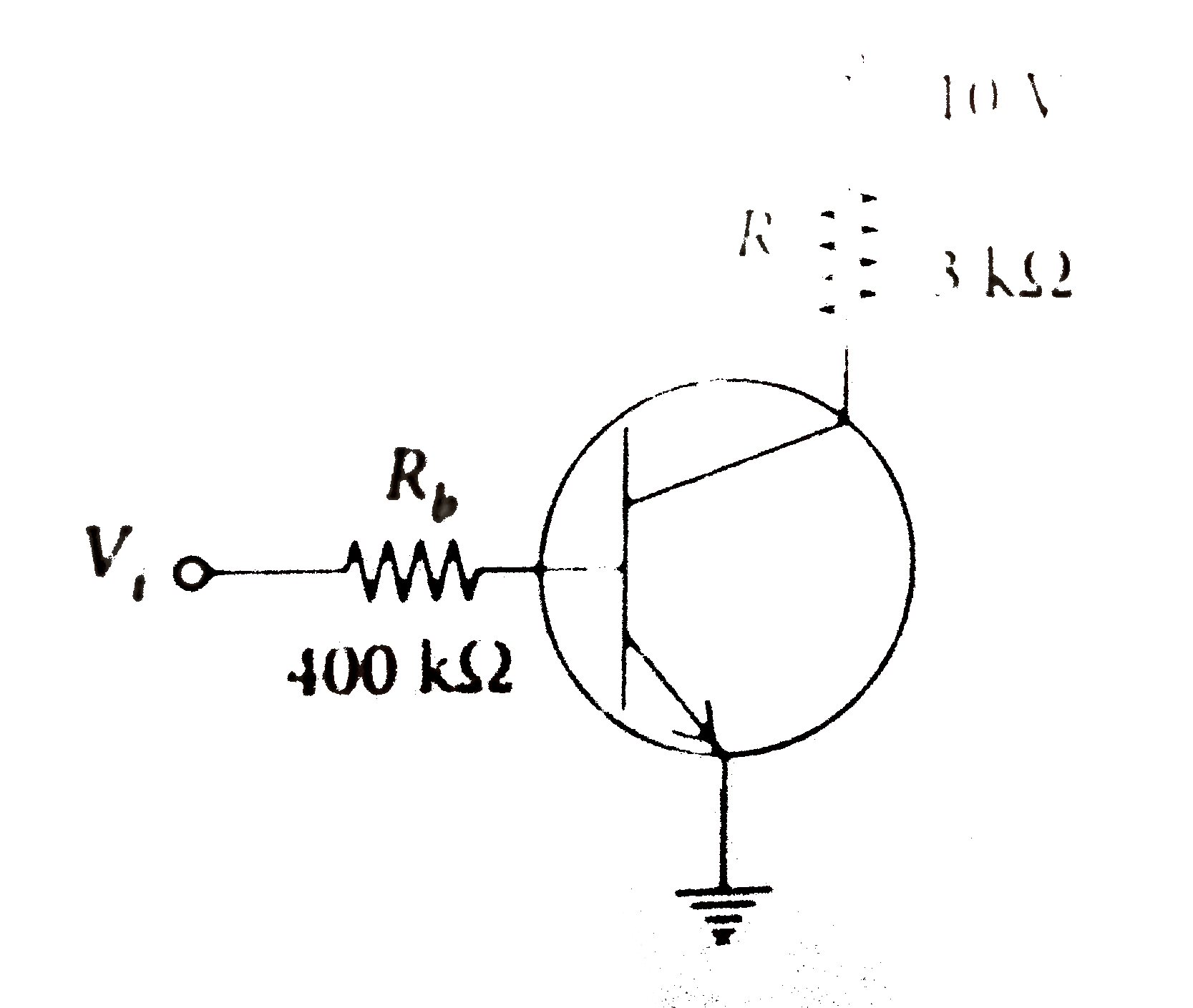 Aβ=110BIb=25μACIc=3.33mADboth (A) and (C )
An NPN-transistor circuit is arranged as shown in figure. It is
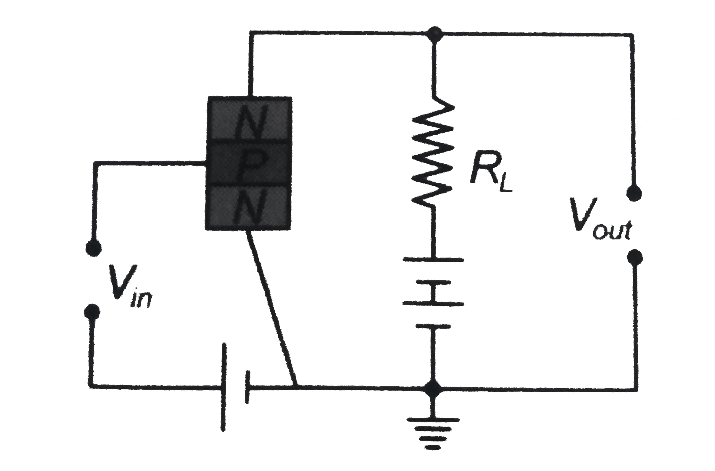 View Solution
In the circuit shown in figure value of VR is
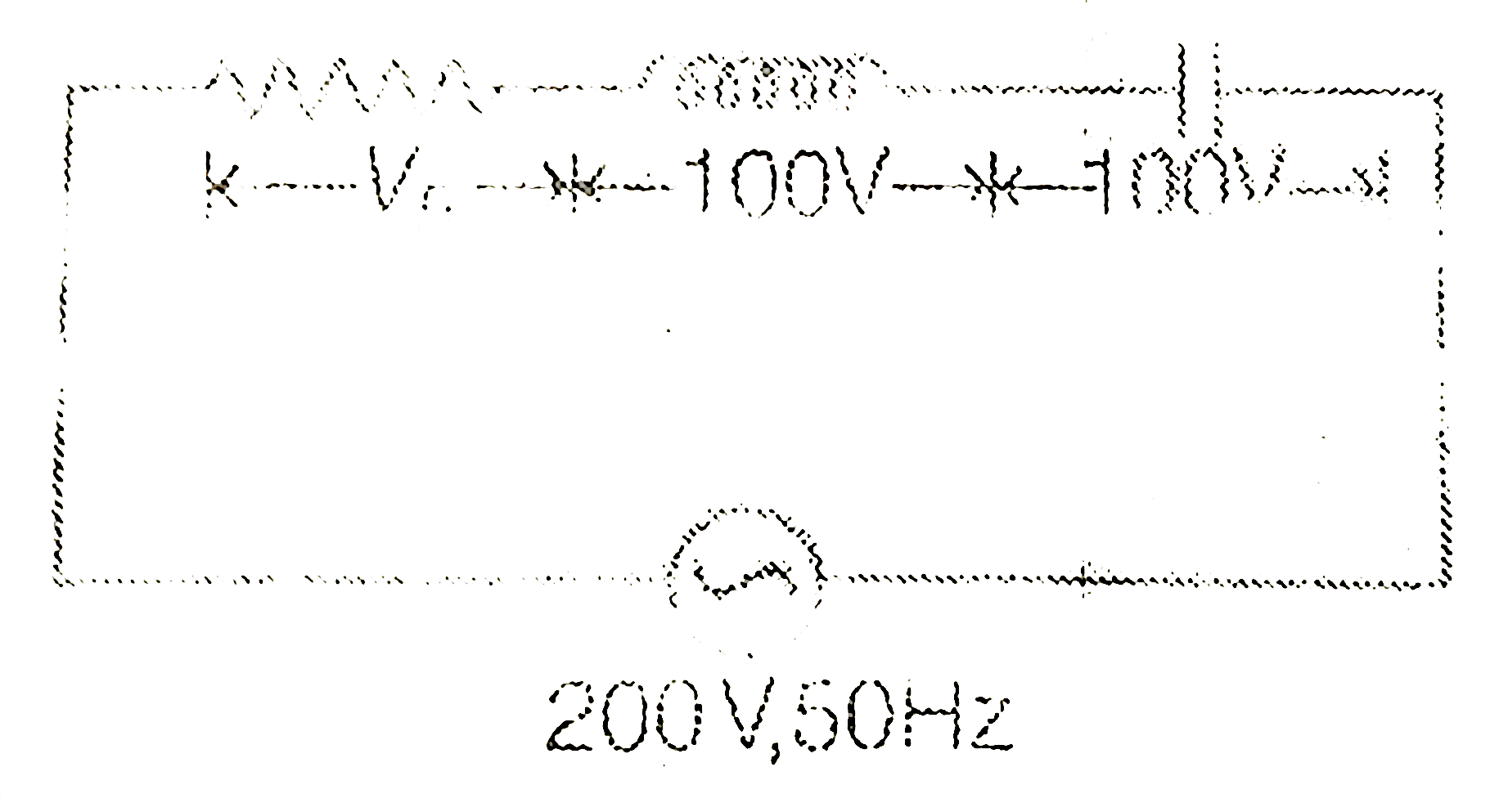 View Solution
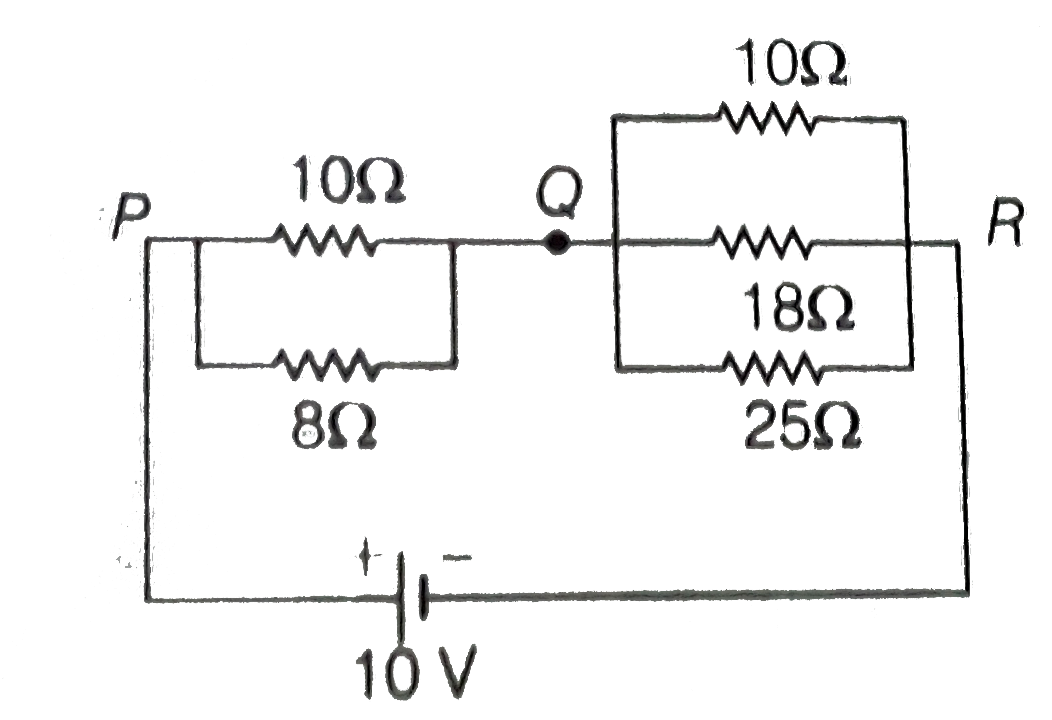
Find VP−VQ in the circuit shown in figure.
 View Solution
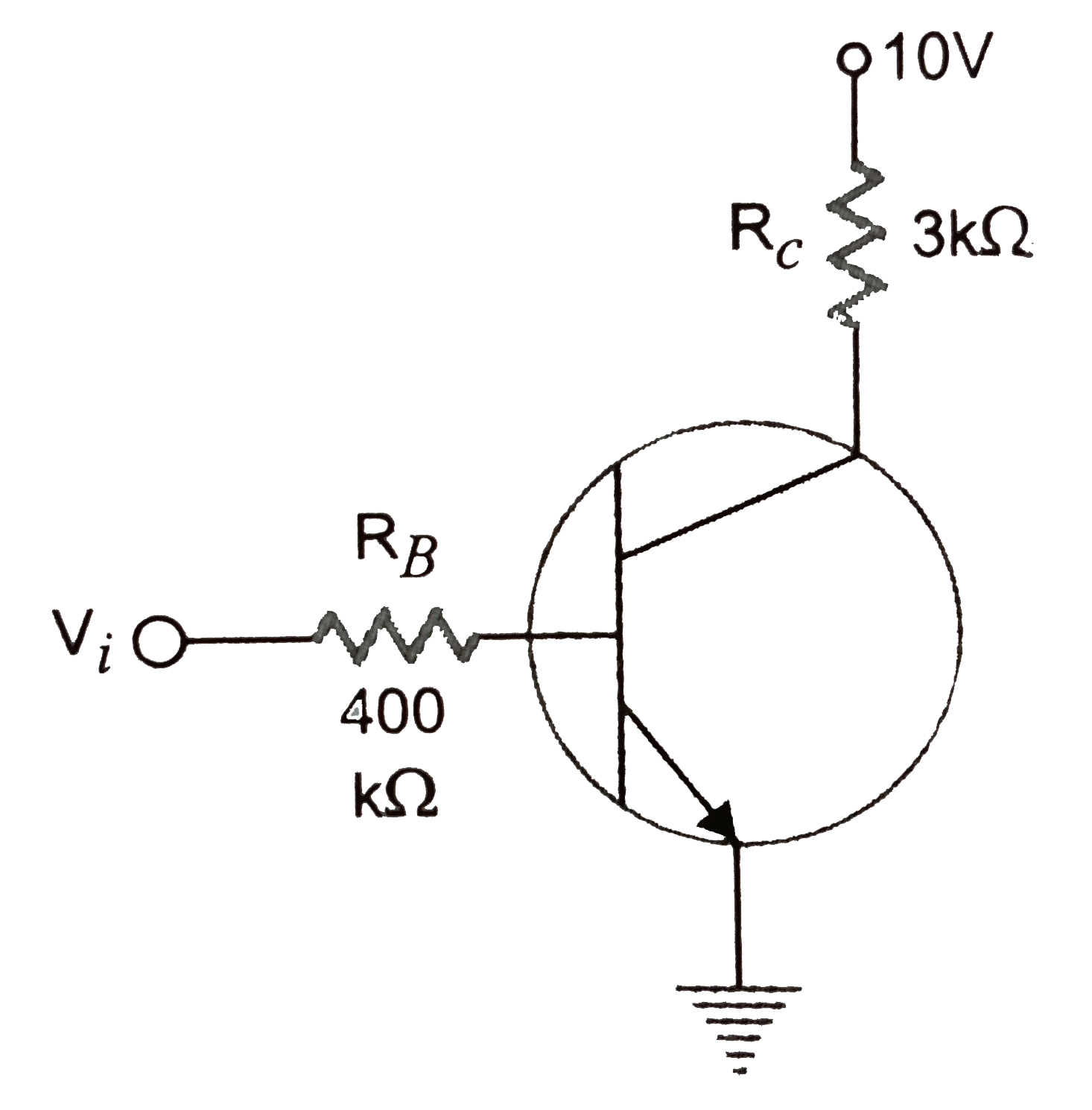
In the circuit shown in Fig. when the input voltage of the base resistance is 10V,Vbe is zero and Vce is also zero. Find the values of I,I and β.
 View Solution
The potential difference between points A and B in the circuit shown in fig. 5.317 is 16V. Then
 View Solution
Draw the diagram of the circuit arangement used for studying the 'input' and the 'output' characteristics of an n-p-n transistor inits CE configuration. Briefly explain how these two types of characteristics are obtained and draw these characteristics.
(b) 'Define' the terms (i) Input resistance, (ii) Output resistance , (iii) Current amplification factor, for a given transistor.View SolutionDraw the typical input and output characterisitics of an n-p-n transistor in CE configurtion . Show how these characteristic can be used to determine (a) the input resistance (r1) and (b) current amplification factor (β).
View Solution

