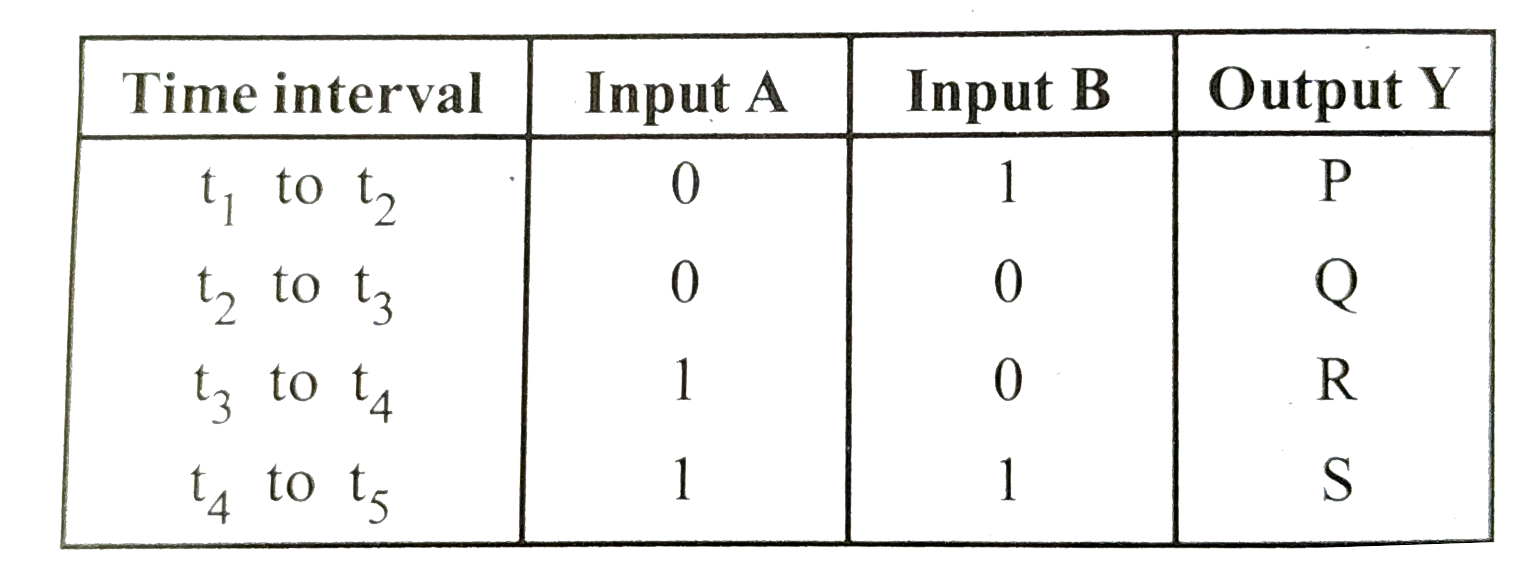
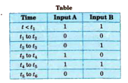
The inputs and outputs for different time intervals are given below for NAND gate
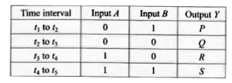
The value taken by P, Q, R, S are respectively
A
1,1,1,0
B
0,1,0,1
C
0,1,0,0
D
1,0,1,1
Video Solution
Text Solution
The correct Answer is:A
Truth table for NAND gate

|
Updated on:21/07/2023
Topper's Solved these Questions
- BOOK - MTG GUIDECHAPTER - ELECTRONIC DEVICESEXERCISE - CHECK YOUR BEET VITALS25videos
ELECTRONIC DEVICES
- BOOK - MTG GUIDECHAPTER - ELECTRONIC DEVICESEXERCISE - AIPMT/NEET (MCQs)42videos
ELECTRONIC DEVICES
- BOOK - MTG GUIDECHAPTER - ELECTRONIC DEVICESEXERCISE - AIPMT/NEET (MCQs)42videos
ELECTRONIC DEVICES
- BOOK - MTG GUIDECHAPTER - ELECTROMAGNETIC WAVESEXERCISE - AIPMT/NEET(MCQs)15videos
ELECTROMAGNETIC WAVES
- BOOK - MTG GUIDECHAPTER - ELECTROSTATICSEXERCISE - AIPMT/NEET (MCQ.s)34videos
ELECTROSTATICS
Similar Questions
Knowledge Check
- Question 1 - Select One
Given below are symbols for some gates. The OR gate and the AND gate, respectively are
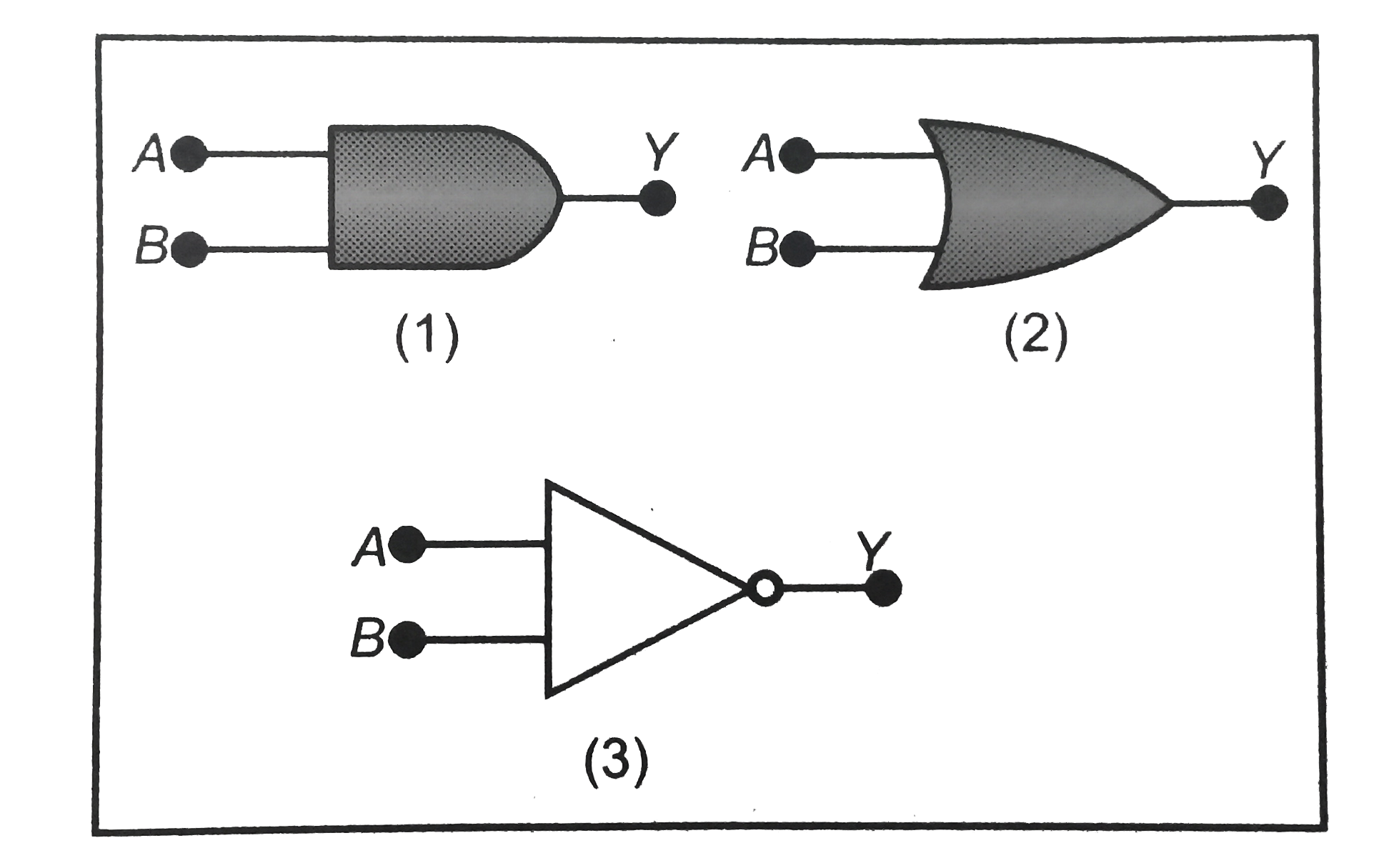 A1 and 3B2 and 3C1 and 2D2 and 1
 - Question 2 - Select One
Given below are symbols for some logic gates :-
_E01_343_Q01.png)
The XOR gate and NOR gate respectively are :-A(a) and (b)B(b) and (c)C(c) and (d)D(a) and (d) - Question 3 - Select One
Given below are four logic tage symboles. Those for OR,NOR and NAND are respectively:
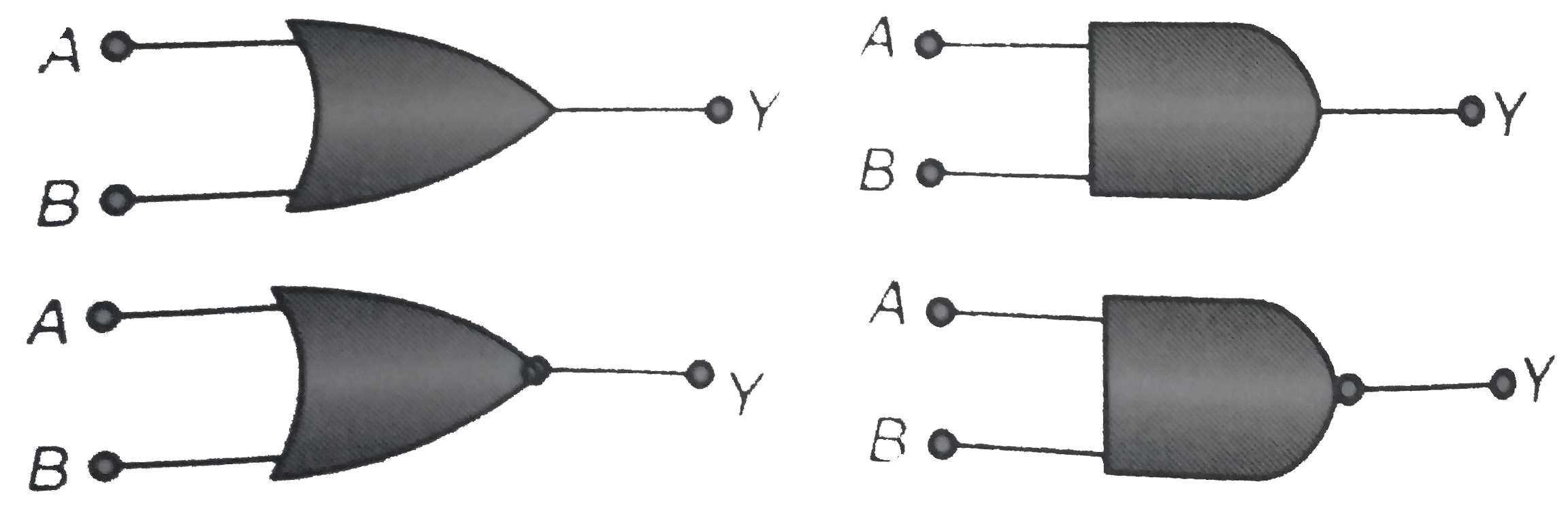 A1,4,3B4,1,2C1,3,4D4,2,1
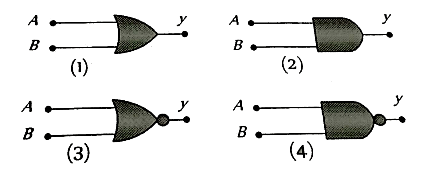
Given below are four logic gates symbol (figure). Those for OR, NOR and NAND are respectively
View SolutionThe symbolic representation of four logic gates are given below :

The logic symbols for OR, NOT and NAND gates are respectively :-View SolutionGiven below are four logic gate symbol (figure). Those for OR, NOR and NAND are respectively
 View Solution
If p→(q∧r) is false, then the truth values of p,q and r are respectively
View SolutionIf the Output of two NAND gates is given to input of a NAND gate. Then the truth table will be of
View Solution


