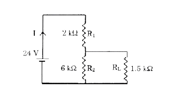
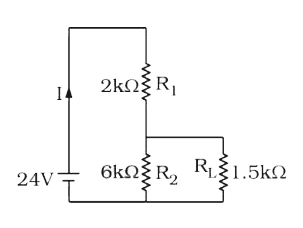
The circuit as shown in the figure is equivalent to

A
AND gate
B
NOR gate
C
OR gate
D
NAND gate
Video Solution
Text Solution
The correct Answer is:D
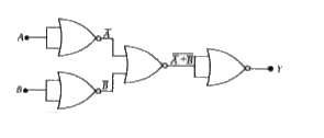
Y=¯¯¯¯¯¯¯¯¯¯¯¯¯¯¯¯¯¯¯¯¯¯¯¯¯¯¯A+¯¯¯B+¯¯¯A+¯¯¯B=¯¯¯¯¯¯¯¯A.B
It is a Boolean expression for NAND gate.
|
Updated on:21/07/2023
Topper's Solved these Questions
- BOOK - MTG GUIDECHAPTER - ELECTRONIC DEVICESEXERCISE - CHECK YOUR BEET VITALS25videos
ELECTRONIC DEVICES
- BOOK - MTG GUIDECHAPTER - ELECTRONIC DEVICESEXERCISE - AIPMT/NEET (MCQs)42videos
ELECTRONIC DEVICES
- BOOK - MTG GUIDECHAPTER - ELECTRONIC DEVICESEXERCISE - AIPMT/NEET (MCQs)42videos
ELECTRONIC DEVICES
- BOOK - MTG GUIDECHAPTER - ELECTROMAGNETIC WAVESEXERCISE - AIPMT/NEET(MCQs)15videos
ELECTROMAGNETIC WAVES
- BOOK - MTG GUIDECHAPTER - ELECTROSTATICSEXERCISE - AIPMT/NEET (MCQ.s)34videos
ELECTROSTATICS
Similar Questions
Knowledge Check
- Question 1 - Select One
The circuit as shown in figure is equivalent to
 ANOR gateBOR gateCAND gateDNAND gate
 - Question 2 - Select One
The circuit as shown in figure is equivalent to
 AOR gateBNOR gateCNAND gateDAND gate
 - Question 3 - Select One or More
In the circuit shown in the figure,
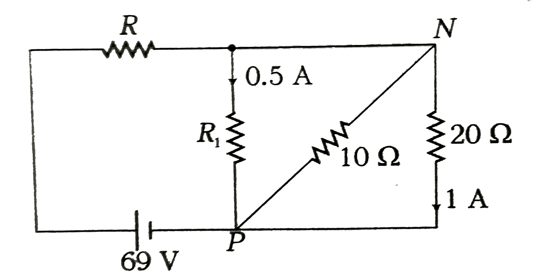 AThe current through NP is 0.5 ABThe value of R1=40ΩCThe value of R =14ΩDsThe potential difference across R = 49 V
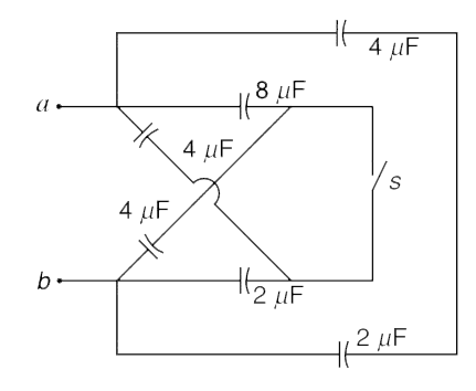
In the circuit shown in the Figure find the equivalent capacitance between points a and b when–
(a) Switch S is open.
(b) Switch S is closed.
 View Solution
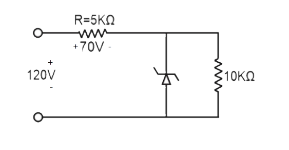
For the circuit shown in the figure :
 View Solution
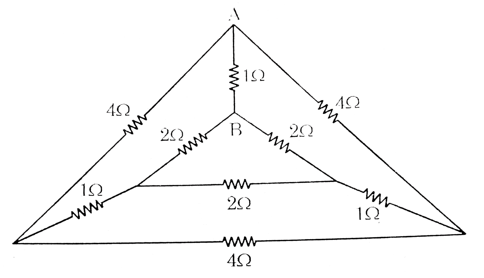
Consider the circuit as shown in figure. The equivalent resistance between A and B is
 View Solution
For the circuit shown in the figure. The equivalent resistance between point A and B for the two cases (i) VA>VB,(ii)VB>VA respectively is……….Ωand……….Ω respectively. (D1andD2 are ideal diodes)
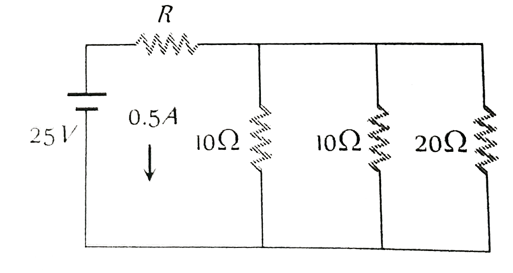
View SolutionIn the circuit as shown in figure the
 View Solution


