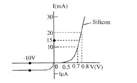
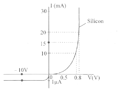
The V-I characteristic of a silicon diode is shown in the Fig. Calculate the resistance of the diode at
VD=−10V
 Solution in Telugu
Considering the diode characteristics as a straight line between I = 10 mA to I = 20 mA passing through the origin, we can calculate the resistance using Ohm.s law.
From the curve at V=- 10V. I =-1μ A
Therefore, rrb = 10V/1 mu A =1.0×10⁷Ω
Topper's Solved these Questions
- BOOK - AAKASH SERIESCHAPTER - SEMICONDUCTOR DEVICESEXERCISE - EXERCISE -I (ENERGY BANDS AND CLASSIFICATION OF SOLIDS )43videos
SEMICONDUCTOR DEVICES
- BOOK - AAKASH SERIESCHAPTER - SEMICONDUCTOR DEVICESEXERCISE - EXERCISE -I (P-N JUNCTION DIODE)35videos
SEMICONDUCTOR DEVICES
- BOOK - AAKASH SERIESCHAPTER - SEMICONDUCTOR DEVICESEXERCISE - Problems (LEVEL-II)7videos
SEMICONDUCTOR DEVICES
- BOOK - AAKASH SERIESCHAPTER - RAY OPTICSEXERCISE - PROBLEMS ( LEVEL-II)50videos
RAY OPTICS
- BOOK - AAKASH SERIESCHAPTER - UNITS AND MEASUREMENTEXERCISE - PRACTICE EXERCISE45videos
UNITS AND MEASUREMENT
Similar Questions
Carbon, silicon and germanium have four valence electrons each. These are characterised by valence and conduction bands separated by energy band gap respectively equal to (Eg)c,(Eg)Si and (Eg)Ge .Which of the following statements is true ?
(a) (Eg)Si<(Eg)Ge<(Eg)C
(b) (Eg)C<(Eg)Ge>(Eg)Si
(c ) (Eg)C>(Eg)SI>(Eg)Ge
(d) (Eg)C=(Eg)Si=(Eg)GeView SolutionThe neutral region formed at P-n junction due to recombination of electrons and holes is
03:52View SolutionA n-type silicon sample of width 4×10⁻³m, thickness 25×10−5m and length 6×10⁻²m carries a current of 4.8 mA when the voltage is applied across the length of the sample. If the free electron density is 1022m−3, then find how much time does it take for the electrons to travel the full length of the sample? Given that charge on an electron e=1.6×10⁻¹⁹C
04:54View SolutionTwo plane mirrors are combined to each other such that one is in y-z plane and the other is in X-z plane. A ray of light travelling along a vector ˆi+ˆi+ˆk is incident on the first mirror. Find the unit vector in the direction of emergent ray after successive reflections through both the mirrors.
03:51View SolutionThe ratio of S.I. unit of universal gravitational constant to C.G.S. unit is
01:34View SolutionThe V-I characteristics of silicon diode is shown in Fig. Calculate the diode resistance in forward bias at V=+0.9V reverse bias V=-3.0V .
02:19View SolutionThe V-I characteristics of a silicon diode is shown in the Fig. . Calculate the resistsnce of the diode at I_(D)=15mA and V_(D)=-10V .
02:02View SolutionThe V-I characteristics of a silicon diode is given in Fig .Calculate the diode resistance in forward bias at V=+2V and V=+1V and reverse bias V=-1V and V=-2V .
02:03View SolutionThe V-I characteristic of a silicon diode is shown in the Fig. Calculate the resistance of the diode at (a) I_(D) = 15 mA and (b) V_(D) = -10 V . .
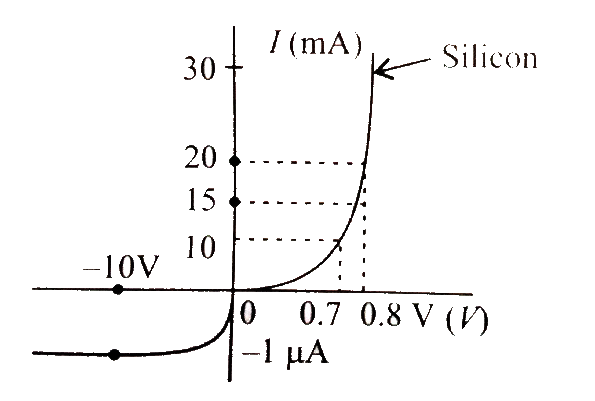
02:02View SolutionThe V-I characteristic of a silicon diode is shown in figure . The resistance of the diode at ID=15 mA is
 03:57View Solution
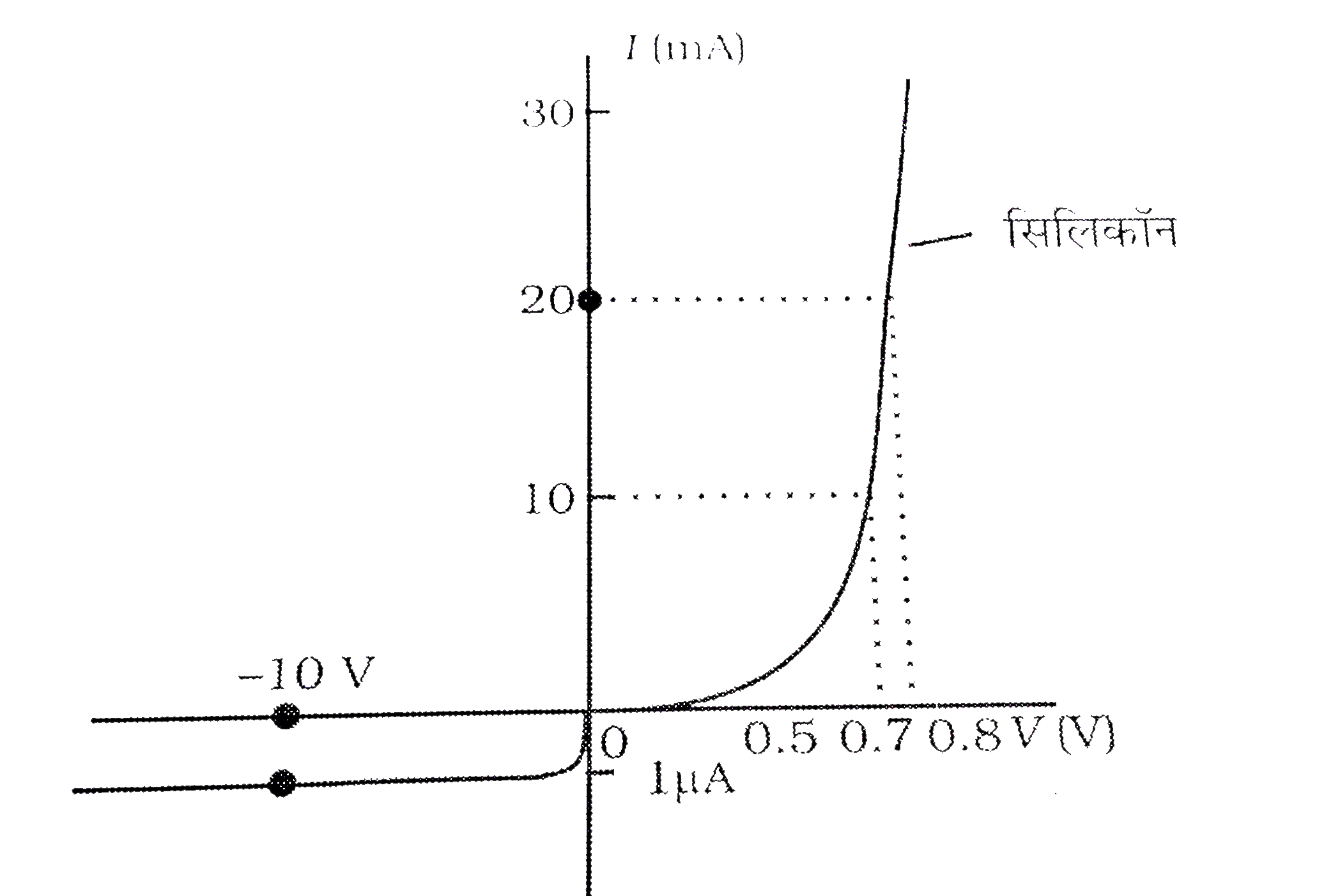
किसी सिलिकॉन डायोड का V−I अभिलाक्षणिक चित्र में दर्शाया गया है। डायोड का प्रतिरोध (a) ID=15mA तथा (b) VD=−10V पर परिकलित कीजिए।
 05:43View Solution
सिलिकॉन डायोड के निम्न प्रेक्षणों से डायोड प्रतिरोध की गणना कीजिए
V=- 10 V पर I =-1 µA,02:50View Solutionसिलिकॉन डायोड के निम्न प्रेक्षणों से डायोड प्रतिरोध की गणना कीजिए
V = 0.8 V पर I= 20 mA तथा V = 0.7 V पर I = 10 mA.03:37View Solutionसिलिकॉन डायोड का V - I अभिलाक्षणिक के लिए अग्र बायस V = +2 वोल्ट पर डायोड प्रतिरोध की गणना कीजिए ? जबकि डायोड धारा का मान 70mAहै
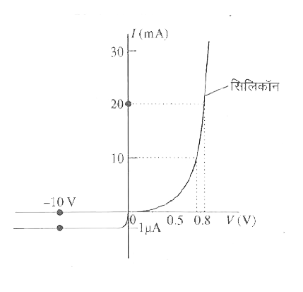
01:44View Solutionकिसी सिलिकॉन डायोड का V-I अभिलाक्षणिक चित्र में दर्शाया गया है| डायोड का प्रतिरोध (a) ID=15mA तथा (b) VD=−10V पर परिकलित कीजिए|
 01:26View Solution
The V-I characteristic of a silicon diode is shown in the figure . Calculate the resistance of the diode at (a) ID=15mA and (b) VD=−10V
 01:59View Solution

