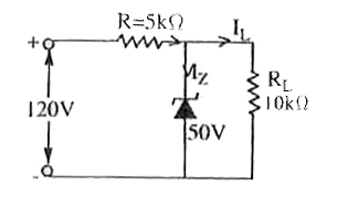
For the circuit shown in Fig. find
the output voltage,
 Solution in Telugu
From the figure
R=5kΩ=5×10³Ω
Input voltage Vin=120V,
zener voltage, VZ=50V
Output voltage. Vz=50V
Topper's Solved these Questions
- BOOK - AAKASH SERIESCHAPTER - SEMICONDUCTOR DEVICESEXERCISE - EXERCISE -I (ENERGY BANDS AND CLASSIFICATION OF SOLIDS )43videos
SEMICONDUCTOR DEVICES
- BOOK - AAKASH SERIESCHAPTER - SEMICONDUCTOR DEVICESEXERCISE - EXERCISE -I (P-N JUNCTION DIODE)35videos
SEMICONDUCTOR DEVICES
- BOOK - AAKASH SERIESCHAPTER - SEMICONDUCTOR DEVICESEXERCISE - Problems (LEVEL-II)7videos
SEMICONDUCTOR DEVICES
- BOOK - AAKASH SERIESCHAPTER - RAY OPTICSEXERCISE - PROBLEMS ( LEVEL-II)50videos
RAY OPTICS
- BOOK - AAKASH SERIESCHAPTER - UNITS AND MEASUREMENTEXERCISE - PRACTICE EXERCISE45videos
UNITS AND MEASUREMENT
Similar Questions
Carbon, silicon and germanium have four valence electrons each. These are characterised by valence and conduction bands separated by energy band gap respectively equal to (Eg)c,(Eg)Si and (Eg)Ge .Which of the following statements is true ?
(a) (Eg)Si<(Eg)Ge<(Eg)C
(b) (Eg)C<(Eg)Ge>(Eg)Si
(c ) (Eg)C>(Eg)SI>(Eg)Ge
(d) (Eg)C=(Eg)Si=(Eg)Ge01:14View SolutionThe neutral region formed at P-n junction due to recombination of electrons and holes is
07:14View SolutionA n-type silicon sample of width 4×10⁻³m, thickness 25×10−5m and length 6×10⁻²m carries a current of 4.8 mA when the voltage is applied across the length of the sample. If the free electron density is 1022m−3, then find how much time does it take for the electrons to travel the full length of the sample? Given that charge on an electron e=1.6×10⁻¹⁹C
02:36View SolutionTwo plane mirrors are combined to each other such that one is in y-z plane and the other is in X-z plane. A ray of light travelling along a vector ˆi+ˆi+ˆk is incident on the first mirror. Find the unit vector in the direction of emergent ray after successive reflections through both the mirrors.
01:57View SolutionThe ratio of S.I. unit of universal gravitational constant to C.G.S. unit is
02:23View SolutionFind output y in the folowing circuit Fig.
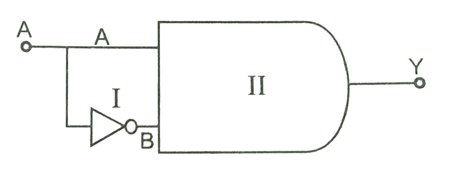 .View Solution
The output of the given circuit in Fig.
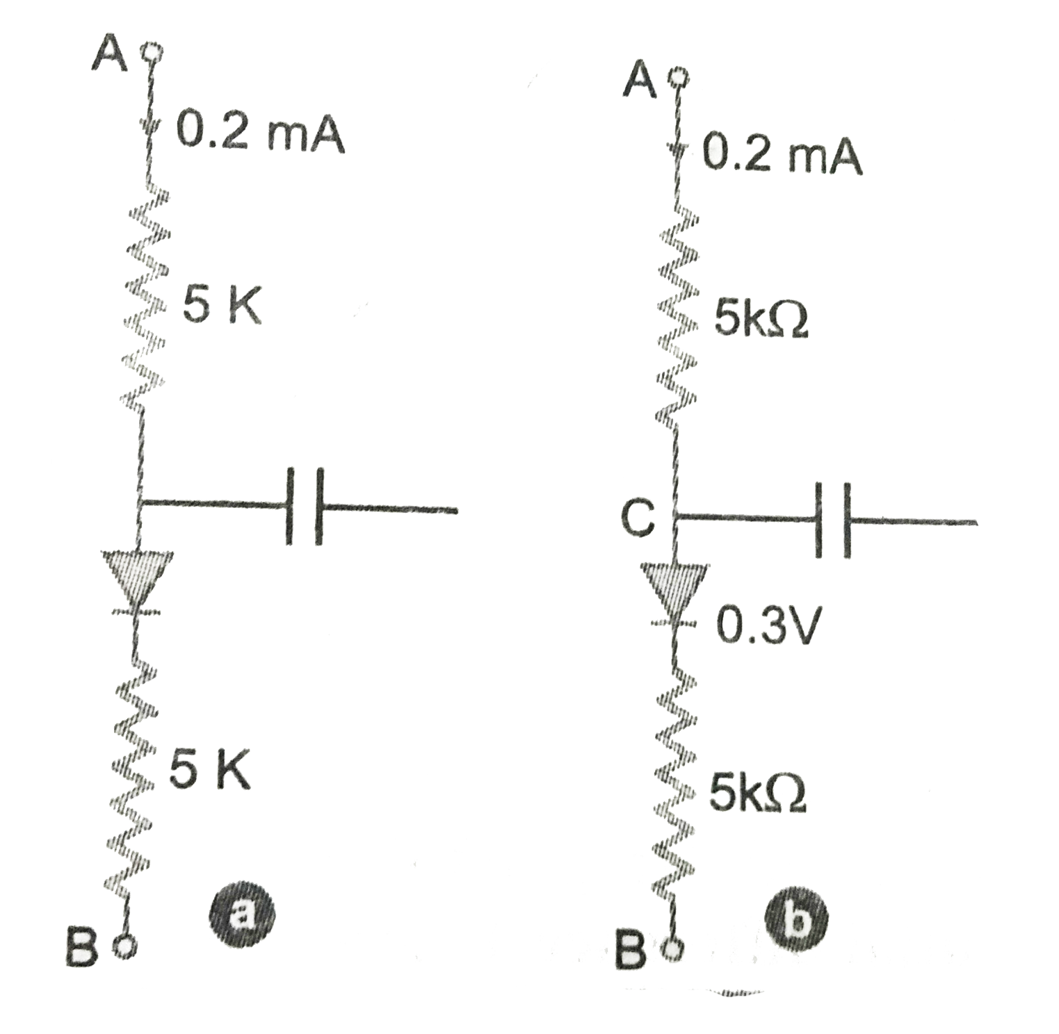 01:57View Solution
Fig, shows a logic gate circuit with two input A and B and the output C. The voltage wave form of A, B and C are as shown in Fig.The logic gate circuit is
05:44View SolutionThe Boolean expression of the output Y of the inputs A and B for the circuit shown in the fig. .
03:00View SolutionThe output of the given circuit in Fig.
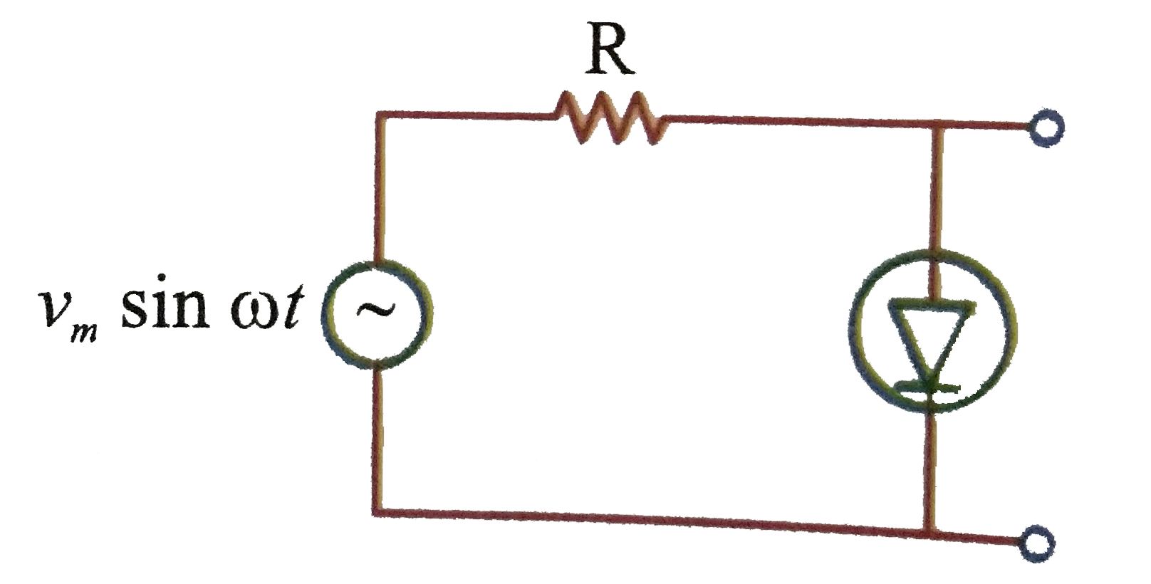 .04:04View Solution
A full wave rectifier circuit along with the input and output voltages is shown in the figure
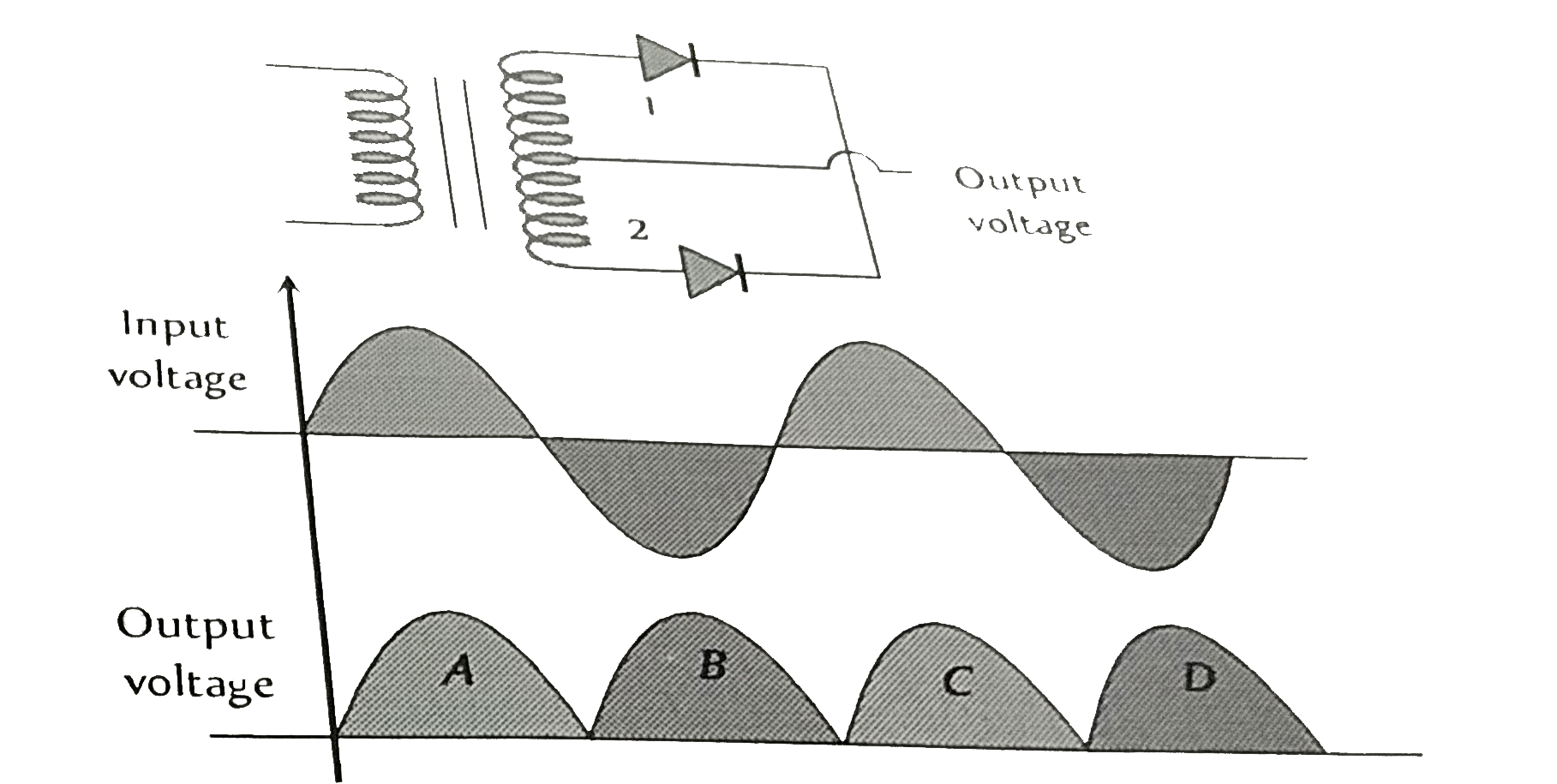
The contribution to output voltage from diode – 2 isView SolutionThe Boolean expression of the output Y of the inputs A and B for the circuit shown in the fig.
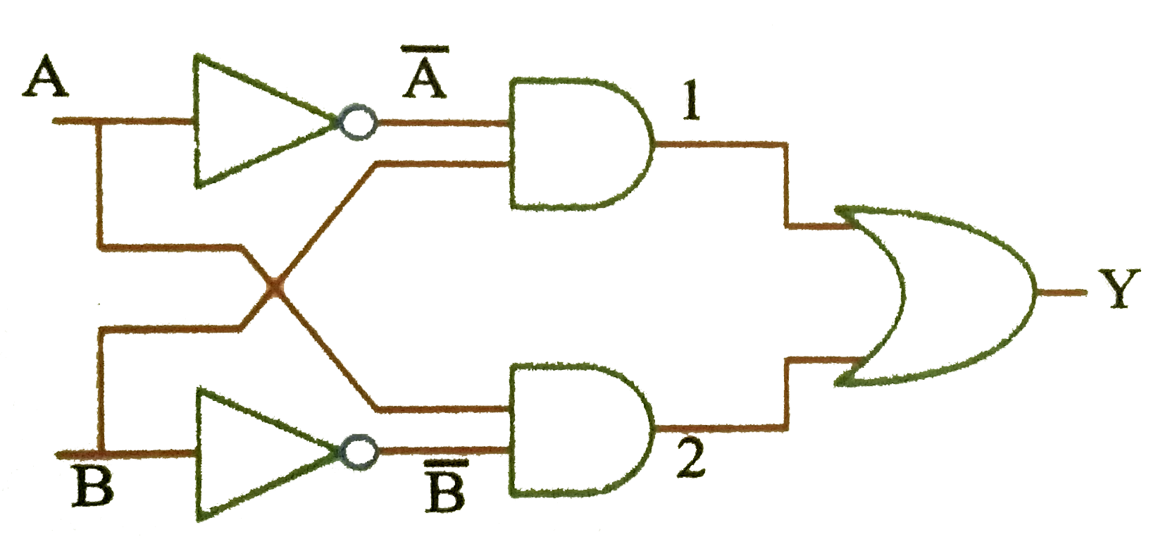 .03:06View Solution
The output of the given circuit in Fig.
02:07View SolutionIn the circuit shown in figure the maximum output voltage
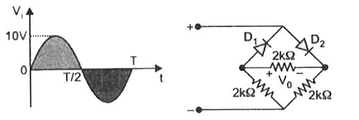 View Solution
एक तार्किक परिपथ को चित्र में दर्शाया गया है। परिपथ से निर्गत F किससे प्रदर्शित होगा
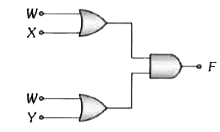 View Solution

