In a properly biased transistor-
Both depletion layers are equally large
Both depletion layers are equally small
Emitter base depletion layer is large but base collector depletion layer is small
Emitter base depletion layer is small but base collector depletion layer is large
The correct Answer is:D
To solve the question regarding the behavior of a properly biased transistor, we can follow these steps:
1. Identify the Transistor Configuration:
- Recognize that the question pertains to a bipolar junction transistor (BJT), which has three regions: emitter, base, and collector.
2. Understand Biasing Conditions:
- In a properly biased transistor, the emitter-base junction is forward-biased, and the base-collector junction is reverse-biased.
3. Draw the Diagram:
- Sketch a simple diagram of the transistor showing the emitter, base, and collector. Indicate the forward bias on the emitter-base junction and the reverse bias on the base-collector junction.
4. Analyze the Depletion Layers:
- In a forward-biased junction (emitter-base), the depletion layer is small because the majority carriers are pushed into the junction.
- In a reverse-biased junction (base-collector), the depletion layer is large because the majority carriers are pulled away from the junction, widening the depletion region.
5. Evaluate the Options:
- Option 1: Both depletion layers are equally large. (Incorrect)
- Option 2: Both depletion layers are equally small. (Incorrect)
- Option 3: Emitter-base depletion layer is large but base-collector depletion layer is small. (Incorrect)
- Option 4: Emitter-base depletion layer is small but base-collector depletion layer is large. (Correct)
6. Conclusion:
- The correct answer is Option 4: "Emitter-base depletion layer is small but base-collector depletion layer is large."
- Recognize that the question pertains to a bipolar junction transistor (BJT), which has three regions: emitter, base, and collector.
- In a properly biased transistor, the emitter-base junction is forward-biased, and the base-collector junction is reverse-biased.
- Sketch a simple diagram of the transistor showing the emitter, base, and collector. Indicate the forward bias on the emitter-base junction and the reverse bias on the base-collector junction.
- In a forward-biased junction (emitter-base), the depletion layer is small because the majority carriers are pushed into the junction.
- In a reverse-biased junction (base-collector), the depletion layer is large because the majority carriers are pulled away from the junction, widening the depletion region.
- Option 1: Both depletion layers are equally large. (Incorrect)
- Option 2: Both depletion layers are equally small. (Incorrect)
- Option 3: Emitter-base depletion layer is large but base-collector depletion layer is small. (Incorrect)
- Option 4: Emitter-base depletion layer is small but base-collector depletion layer is large. (Correct)
- The correct answer is Option 4: "Emitter-base depletion layer is small but base-collector depletion layer is large."
Topper's Solved these Questions
- SEMICONDUCTOR ELECTRONICS: MATERIALS, DEVICES AND SIMPLE CIRCUITSBOOK - AAKASH INSTITUTE ENGLISHCHAPTER - SEMICONDUCTOR ELECTRONICS: MATERIALS, DEVICES AND SIMPLE CIRCUITSEXERCISE - Assignment (Section -B (Objective type question (one option is correct))
29 Videos
- SEMICONDUCTOR ELECTRONICS: MATERIALS, DEVICES AND SIMPLE CIRCUITSBOOK - AAKASH INSTITUTE ENGLISHCHAPTER - SEMICONDUCTOR ELECTRONICS: MATERIALS, DEVICES AND SIMPLE CIRCUITSEXERCISE - Assignment (Section -C(Linked comprehension type question))
3 Videos
- SEMICONDUCTOR ELECTRONICS: MATERIALS, DEVICES AND SIMPLE CIRCUITSBOOK - AAKASH INSTITUTE ENGLISHCHAPTER - SEMICONDUCTOR ELECTRONICS: MATERIALS, DEVICES AND SIMPLE CIRCUITSEXERCISE - Try yourself
20 Videos
- SEMICONDUCTOR ELECTRONICS (MATERIAL, DEVICES AND SIMPLE CIRUITS )BOOK - AAKASH INSTITUTE ENGLISHCHAPTER - SEMICONDUCTOR ELECTRONICS (MATERIAL, DEVICES AND SIMPLE CIRUITS )EXERCISE - Assignment SECTION - D (Assertion & reason type Question)
10 Videos
- SYSTEM OF PARTICLES AND ROTATIONAL MOTIONBOOK - AAKASH INSTITUTE ENGLISHCHAPTER - SYSTEM OF PARTICLES AND ROTATIONAL MOTIONEXERCISE - Try Yourself
63 Videos
Similar Questions
Knowledge Check
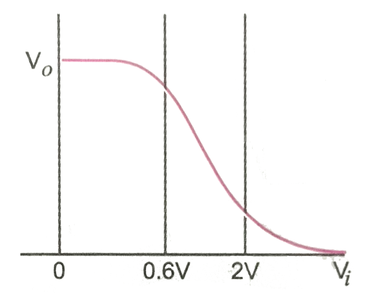
Fig.shows that transfer characteristics of a base biased CE transistor. Which of the following statements are true?
 AAt Vi=1V, it can be used as an amplifierBAt Vi=0.5V, it can be used as a switch turned offCAt Vi=2.5V, it can be used as a switch turned onDAll of these
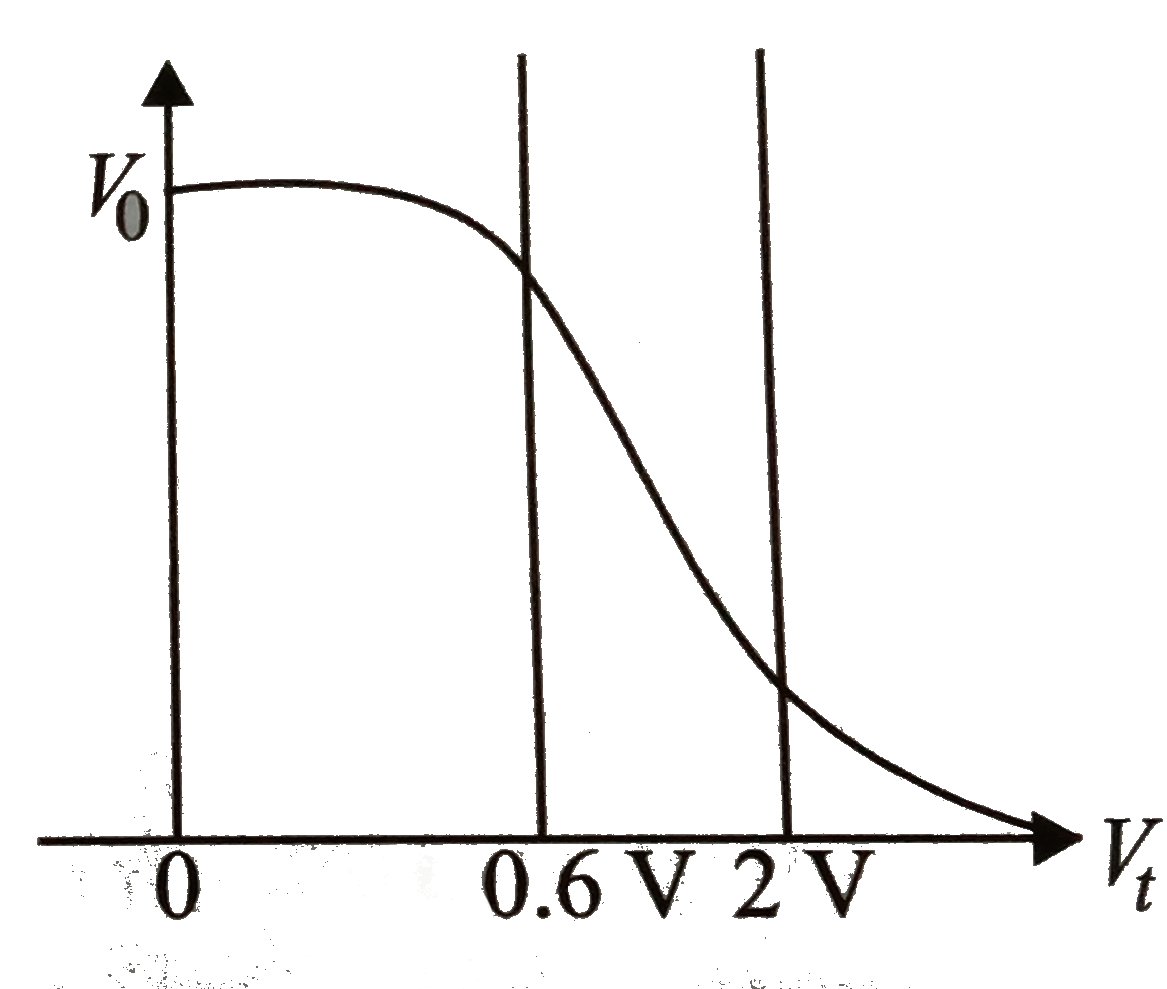
The transfer characteristics of a base biased common emitter transistor is shown in the figure. Which of the following statements are true?

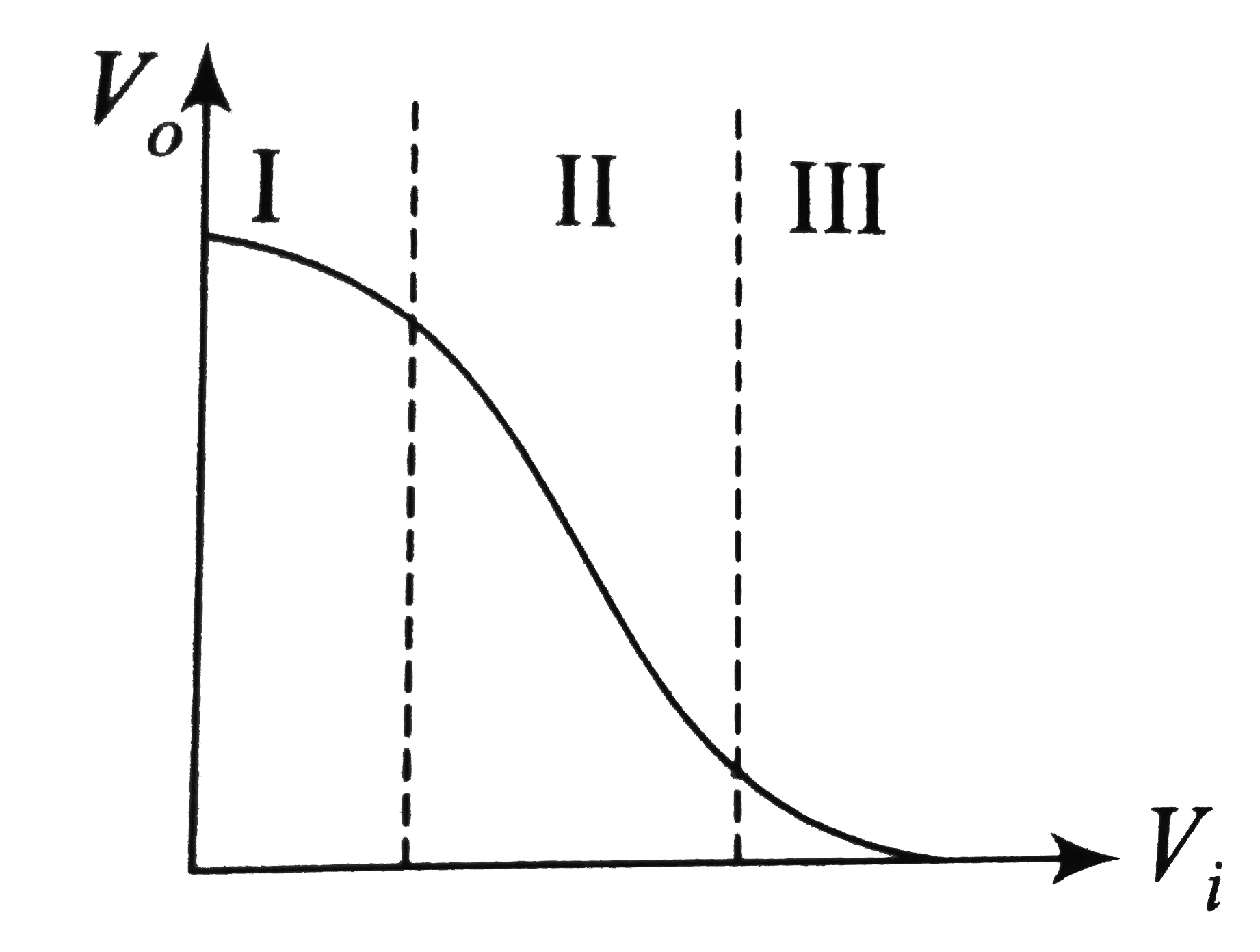
View SolutionTransfer characterstics [output voltage (Vo) vs. input voltage (Vi)] for a base biased transistor in CE configuration is as shown in the figure. For using transfor as a which, it is used

View SolutionIn a normal operation of a transistor,
(i) base-emitter junction is forward-biased
(ii) base-collector junction is forward-biased
(iii) base-emitter junction is reverse-baised
(iv) base-collector junction is reverse-biased
View SolutionDraw the tramsfer characteristic curve of a base biased transistor in CE configuration. Explain clearly how the active region of the Vo versus Vi curve in a transistor is used as an amplifier.
View SolutionIn a normal operation of a transistor,
View SolutionThe concentration of impurities in a transistor is
View SolutionIn a normal operation of a transistor,
View Solution
