Draw the circuit symbol of PNP transistor.
To draw the circuit symbol of a PNP transistor, follow these steps:
1. Understand the Structure: Recognize that a PNP transistor consists of three layers: P-type, N-type, and P-type. The three terminals are the emitter (P), base (N), and collector (P).
2. Draw the Circle: Start by drawing a circle. This circle represents the body of the transistor.
3. Indicate the Terminals: Inside the circle, you will need to indicate the three terminals:
- Draw a line from the top of the circle and label it as the Emitter (E).
- Draw a line from the bottom of the circle and label it as the Collector (C).
- Draw a line from the side of the circle and label it as the Base (B).
4. Draw the Arrow: To indicate that it is a PNP transistor, draw an arrow on the emitter line pointing towards the base. This arrow signifies the direction of conventional current flow (from P to N).
5. Label the Terminals: Clearly label each terminal (Emitter, Base, Collector) to avoid any confusion.
Final Circuit Symbol:
- The final symbol should look like a circle with three lines extending from it, one for each terminal, and an arrow on the emitter line pointing towards the base.
- Draw a line from the top of the circle and label it as the Emitter (E).
- Draw a line from the bottom of the circle and label it as the Collector (C).
- Draw a line from the side of the circle and label it as the Base (B).
- The final symbol should look like a circle with three lines extending from it, one for each terminal, and an arrow on the emitter line pointing towards the base.
Topper's Solved these Questions
- QUESTION BANK 2021BOOK - NAVNEET PUBLICATION - MAHARASHTRA BOARDCHAPTER - QUESTION BANK 2021EXERCISE - Semiconductors Devices (Short Answer I (SA1) ( 2 MARKS Each ) )
7 Videos
- QUESTION BANK 2021BOOK - NAVNEET PUBLICATION - MAHARASHTRA BOARDCHAPTER - QUESTION BANK 2021EXERCISE - Semiconductors Devices ( Short Answer II (SA2) ( 3 MARKS Each ) )
6 Videos
- QUESTION BANK 2021BOOK - NAVNEET PUBLICATION - MAHARASHTRA BOARDCHAPTER - QUESTION BANK 2021EXERCISE - Semiconductors Devices (MCQ’S (1 Mark Each) )
8 Videos
- MULTIPLE CHOICE QUESTIONSBOOK - NAVNEET PUBLICATION - MAHARASHTRA BOARDCHAPTER - MULTIPLE CHOICE QUESTIONSEXERCISE - Communication Systems
6 Videos
- SHORT ANSWER QUESTIONSBOOK - NAVNEET PUBLICATION - MAHARASHTRA BOARDCHAPTER - SHORT ANSWER QUESTIONSEXERCISE - Assignments
3 Videos
Similar Questions
Knowledge Check
The symbol of p-n-p transistor is
A B
B C
C D
D
Draw the symbol of a p-n-p transistor. Show the biasing of a p-n-p transistor and explain the transistor action.
View SolutionDraw a circuit diagram of a transistor amplifier in CE configuration. Define the terms (i) Input resistance and (ii) Current amplification factor. How are these determined using input and output characteristics?
View SolutionDraw circuit diagram for n-p-n transistor to draw input and output characteristics in common base configuration. Draw the input and ouput curves and explain them.
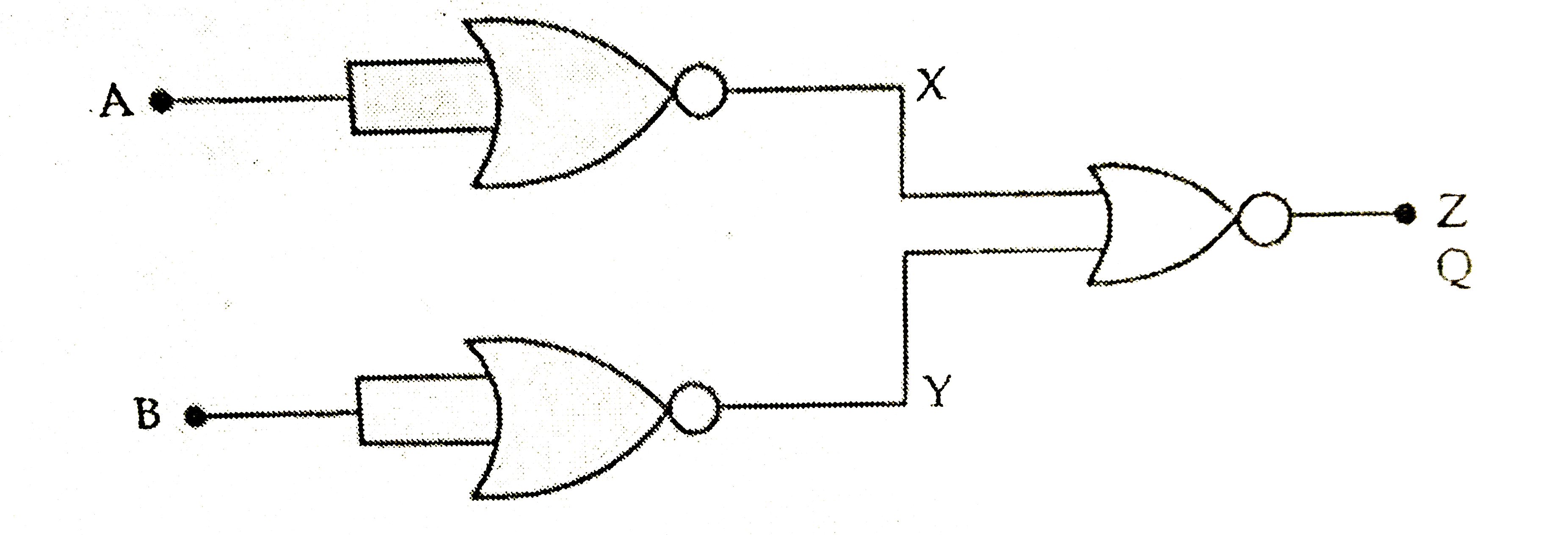
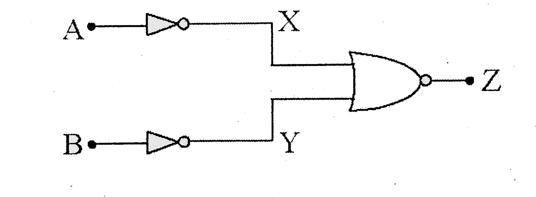
View SolutionYou are given a circuit below. Write its truth table. Hence, identify the logic operation carried out by this circuit. Draw the logic symbol of the gate it corresponds to.

View Solution
You are given a circuit below. Write its truth table. Hence, identify the logic operation carried out by this circuit. Draw the logic symbol of the gate it corresponds to.
View SolutionDraw circuit symbols for (a) fixed resistance (b) variable resistance (c) a cell (d) a battery of three cells (e) an open switch (f) a closed switch.
View SolutionDraw the logic symbol of NAND gate and give its Truth table
View Solution
