What do you understand by logic gate? Discuss, how is an OR gate is realized from its electronic circuit. Give its circuit symbol and truth table.
Text Solution
As shown in figure a two input OR gate can be realised by using two ideal diodes D1andD2 and a resistor R. The negative terminal of the battery is grounded (i.e. it is at zero volt) and corresponds to the 0 state and the positive terminal (which is at say 5V) corresponds to the 1 state.
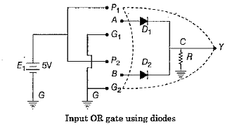
The following four cases are possible:
(i) When A = 0 and B = 0, both the diodes are connected to earth (0V). They do not conduct. Output across R is zero, i.e. Y = 0.
(ii) When A = 0 and B = 1, D1 is connected to earth. It does not conduct. D2 is connected to 5V, it gets forward biased and conducts. Voltage drop across D2 is zero and the full voltage of 5 V appears across R. So, Y = 1.
(iii) When A = 1 and B = 0 D1 gets forward biased and D2 does not conduct. Voltage drop across R is again 5V. So, Y = 1.
(iv) When A = 1 and B = 1, both D1andD2 get forward biased and conduct current. But D1andD2 are in parallel. Voltage drop across R is still 5V.
So, Y = 1.
Hence, the circuit shown in figure above satisfies the truth-table of OR gate.
|
Similar Questions
Knowledge Check
For given logic gate circuit, which truth table is right.
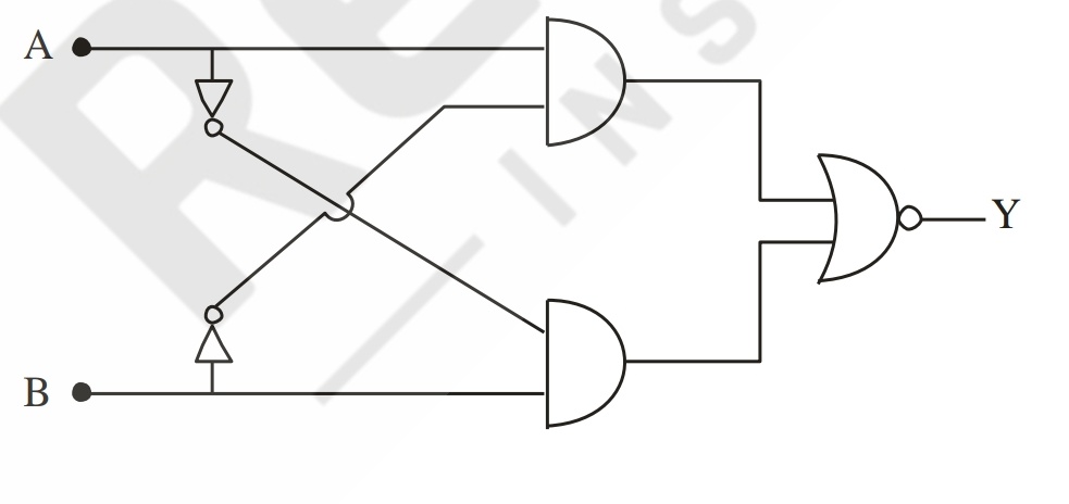 A
A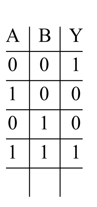 B
B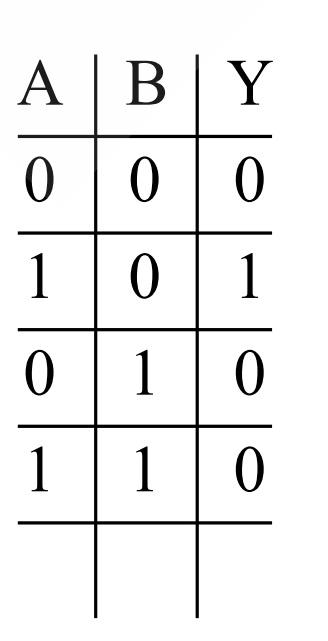 C
C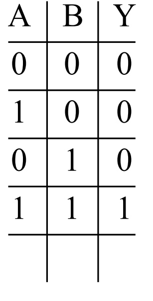 D
D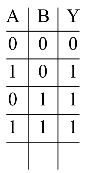
A logic gate and its truth table are shown below
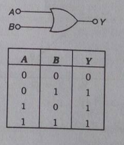
The gate is :ANORBANDCORDNOTA logic gate and its truth table are shown below

The gate is :ANORBANDCORDNOT
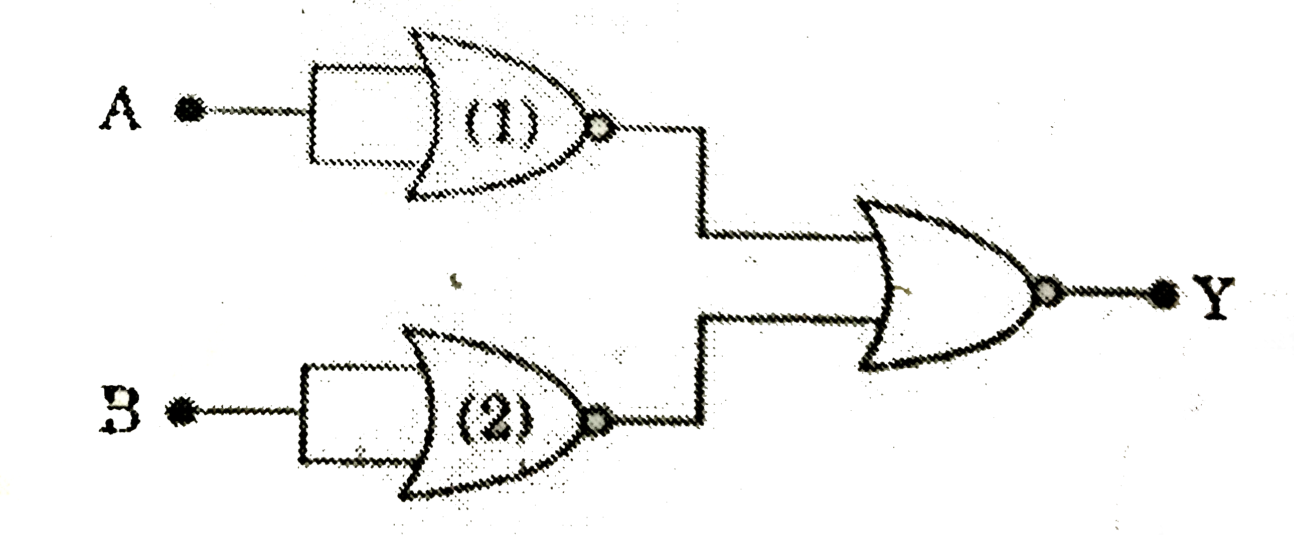
The inputs A and B are inverted by using two NOT gates and their outputs are fed to the NOR gate as shown:
Analyse the action of the gates (1) and (2) and identify the logic gate of the complete circuit so obtained. Give its symbol and the truth table.
View SolutionThe output of a 2-input AND gate is fed to a NOT gate. Give the name of the combination and its logic symbol. Write down its truth table.
View SolutionThe output of a 2-input AND gate is fed to a NOT gate. Give the name of the combination and its logic symbol. Write down its truth table.
View SolutionThe output of and AND gate is connected to both the inputsof a NAND gate. Draw the logic circuit of this combinationn of gates and write its truth table.
View SolutionDraw the logic symbol of NAND gate and give its Truth table
View Solution
