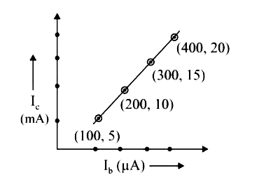
The transfer characteristic curve of a transistor, having input and output resistance 100Ωand100kΩ respectively, is shown in the figure. The Voltage and Power gain, are respectively:

5×104,2.5×106
2.5×104,2.5×106
5×104,5×106
5×104,5×105
The correct Answer is:A
Step by step video & image solution for The transfer characteristic curve of a transistor, having input and output resistance 100Omega and 100kOmega respectively, is shown in the figure. The Voltage and Power gain, are respectively: by Physics experts to help you in doubts & scoring excellent marks in Class 12 exams.
Updated on:21/07/2023Similar Questions
In a common base transitor amplifier, the input and the output resistance area 500Ω and 40kΩ and the emitter current is 1.0mA find the input and the output voltages. Given α=0.95.
View SolutionGraph between output current (Ic) and input current (IB) for common emitter of n−p−n transistor is given in the figure. If input resistance is 100Ω and output resistance is 100Kω. Find out voltage gain and power gain are
_2019_CBT7_E01_019_Q01.png)
View Solution
Knowledge Check
If β,RLandr are the ac current gain, load resistance and the input resistance of a transistor respectively in CE configuration, the voltage and the power gains respectively are
AβRLrandβ2RLrBβrRLandβ2rRLCβRLrandβ(RLr)2DβrRLandβ(rRL)2In common emitter amplifier, the current gain is 62. The collector resistance and input resistance are 5kΩ an 500Ω respectively. If the input voltage is 0.01V, the output voltage is
A0.62VB6.2VC62VD620V
Graph between output current (Ic) and input current (IB) for common emitter of n−p−n transistor is given in the figure. If input resistance is 100Ω and output resistance is 100Kω. Find out voltage gain and power gain are
_2019_CBT7_E01_019_Q01.png)
View SolutionA CE amplifier, has a power gain of 40 dB. The input resistance and output load resistance are 500Ωand2kΩ respectively. Find the value of common - emitter current gain.
[take gain in dB =10log(PoutPin)]
View SolutionPower gain for N−P−N transistor is 10∘, input resistance 100Ω and output resistance 10000Ω. Find out current gain.
View SolutionAn experiment is preformed to determine the I−V characteristics of a Zener diode, which has a protective resistance of R=100Ω, and maximum power of dissipation rating of 1 W. The minimum voltage range of the DC source in the circuit is :-
View SolutionA battery of emf epsilon and internal resistance r is connected across a load resistance RL . The plot between output power and load resistance is shown in the figure. The value of emf epsilon and internal resistance r respectively will
_PHY_E05_112_Q01.png)
View SolutionA transistor is used as an amplifier in CB mode with a load resistance of 5kΩ the current gain of amplifier is 0.98 and the input resistance is 70Ω, the voltage gain and power gain respectively are
View Solution
