Increasing forward voltage in diode, the width of depletion layer is ……..Solution in Gujrati
decreases
increases
fluctuates
does not change
The correct Answer is:A
Step by step video & image solution for Increasing forward voltage in diode, the width of depletion layer is …….. by Physics experts to help you in doubts & scoring excellent marks in Class 11 exams.
Topper's Solved these Questions
- BOOK - ALLEN CHAPTER - SEMICONDUCTORSEXERCISE - Part-3(Exercise-2)49videos
SEMICONDUCTORS
- BOOK - ALLEN CHAPTER - SEMICONDUCTORSEXERCISE - Part-3(Exercise-3)27videos
SEMICONDUCTORS
- BOOK - ALLEN CHAPTER - SEMICONDUCTORSEXERCISE - Part-3(Exercise-4)50videos
SEMICONDUCTORS
- BOOK - ALLEN CHAPTER - PHYSICAL WORLD, UNITS AND DIMENSIONS & ERRORS IN MEASUREMENT EXERCISE - EXERCISE-IV7videos
PHYSICAL WORLD, UNITS AND DIMENSIONS & ERRORS IN MEASUREMENT
- BOOK - ALLEN CHAPTER - WAVES AND OSCILLATIONSEXERCISE - Part-1(Exercise-05)[B]42videos
WAVES AND OSCILLATIONS
Similar Questions
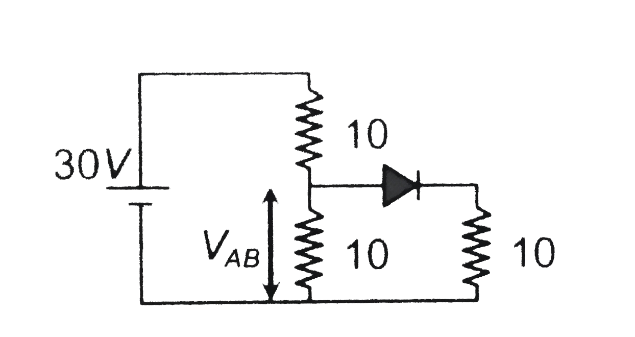
Find VAB
 01:25View Solution
Assertion: Microwave communication is preferred to optical communication
Reason: Microwaves provide large number of channels and bandwidths as compared to optical signals.07:07View SolutionAt absolute zero temperature Si acts as ……..
03:19View SolutionAssertion : Gravitational forces do not depend on the medium between the masses.
Reason : Mediating particle responsible for gravitational force is graviton.01:40View SolutionA string of length 0.4m and mass 10−2kg is clamped at one end . The tension in the string is 1.6N. The identical wave pulses are generated at the free end after regular interval of time , Δt . The minimum value of Δt , so that a constructive interference takes place between successive pulses is
03:02View SolutionIf the forward voltage in a diode is increased, the width of the depletion region-
02:16View Solutionअवक्षय परत की चौड़ाई पर क्या प्रभाव पड़ेगा यदि अग्र दिशिक विभव बढ़ा दी जाये ?
View SolutionIn forward bias the width of depletion layer is
03:14View SolutionIf the forward voltage in p-n junction is increased , the length of depletion layer will
03:02View SolutionThe knee voltage of a p-n junction diode is 0.8 V and the width of the depletion layer is 2muA . The electric field in the depletion layer is
02:10View SolutionWhen reverse bias in a junction diode is increased, the width of depletion layer -
02:44View SolutionIf the forward voltage in a semiconductor is doubled, the width of depletion layer will
03:50View Solutionयदि क्रिस्टल डायोड का अग्र वोल्टेज बढ़ा दिया जाए, तो अवक्षय परत की मोटाई
03:18View SolutionIf the forward voltage in a diode in increased, the width of the depletion region.
02:39View SolutionIf the forward voltage in a diode is increased the width of the depletion region
View SolutionIf the forward voltage in a semiconductor is doubled, the width of depletion layer will
01:56View Solution

