Discuss common emitter characteristics of a transistor.
The graphs between voltages and currents when emitter of a transistor is common to input and output circuits, are known as common emitter characteristics of a transistor.

Circuit diagram to study the common emitter characteristics of n-p-n transistor
Common emitter characteristics are of two types:
(i) Input characteristics: The variation of he base current IB (input) with base emitter 1 voltage VBE at constant collector emitter voltage VCE is called input characteristics.

Keep VCE constant say to 0V. Now change the VBE in steps by using variable resistance R2 and note the corresponding value of the base current (IB). Plot a graph
Between various values of VBE and IB. The curve so obtained is called input characteristic. Now vary VCE to different values say (2V,4V-) corresponding variation of VBE and IB is observed. The collective information from these observations is shown in figure. It is observed that input characteristics are similar to forward bias characteristics of a junction diode.
Input resistance (ri): It is defined as the ratio of small change in base emitter voltage (ΔVBE) to the small change in base current (ΔIB) at constant collector emitter voltage (VCE).
that is ri=(ΔVBEΔIB)VCE
(ii) Out put characteristics: The variation of the collector current IC (output) with collector emitter voltage (VCE) at constant base current (IB) is called output characteristics.Keep the base current (IB) constant say 10μA. Now change the collector emitter voltage (VCE) using variable resistance (R1) and note the corresponding values of collector (IC). The graph between VCE and IC is plotted which is the output characteristic of the transistor. Now fixed IB at different values of (say 20 μA,30μA,) corresponding variation of VCE and IC is observed.
The collective information from these observations is shown in figure.

It is observed that for a given value of base curretn, collector increases with collector emitter voltage.But later collector current becomes constant.
Output resistnace (ra): It is defined as the ratio of small change in collector voltage (ΔVCE) to the small change in collector current (ΔIC) that is
rO=(ΔVCEΔIC)IB
Similar Questions
Draw a circuit diagram to study characteristics of a transistor (pnp or ppn) in common emitter configuration. Draw the sketch of (i) input characterisitics and (ii) output characteristics for this configuration.
View SolutionDraw the circuit diagram for studying the characteristics of a transistor in common emitter configuration. Explain briefly and show how input and output characteristics are drawn.
View Solution
Knowledge Check
In a common-base configuration of a transistor ΔiΔie=0.98, then current gain in common emitter configuration of transistor will be
A49B98C4.9D24.5The base current in common emitter mode of the transistor changes by 10μ(A). If the current gain of the transistor is 50, then change in collector current is
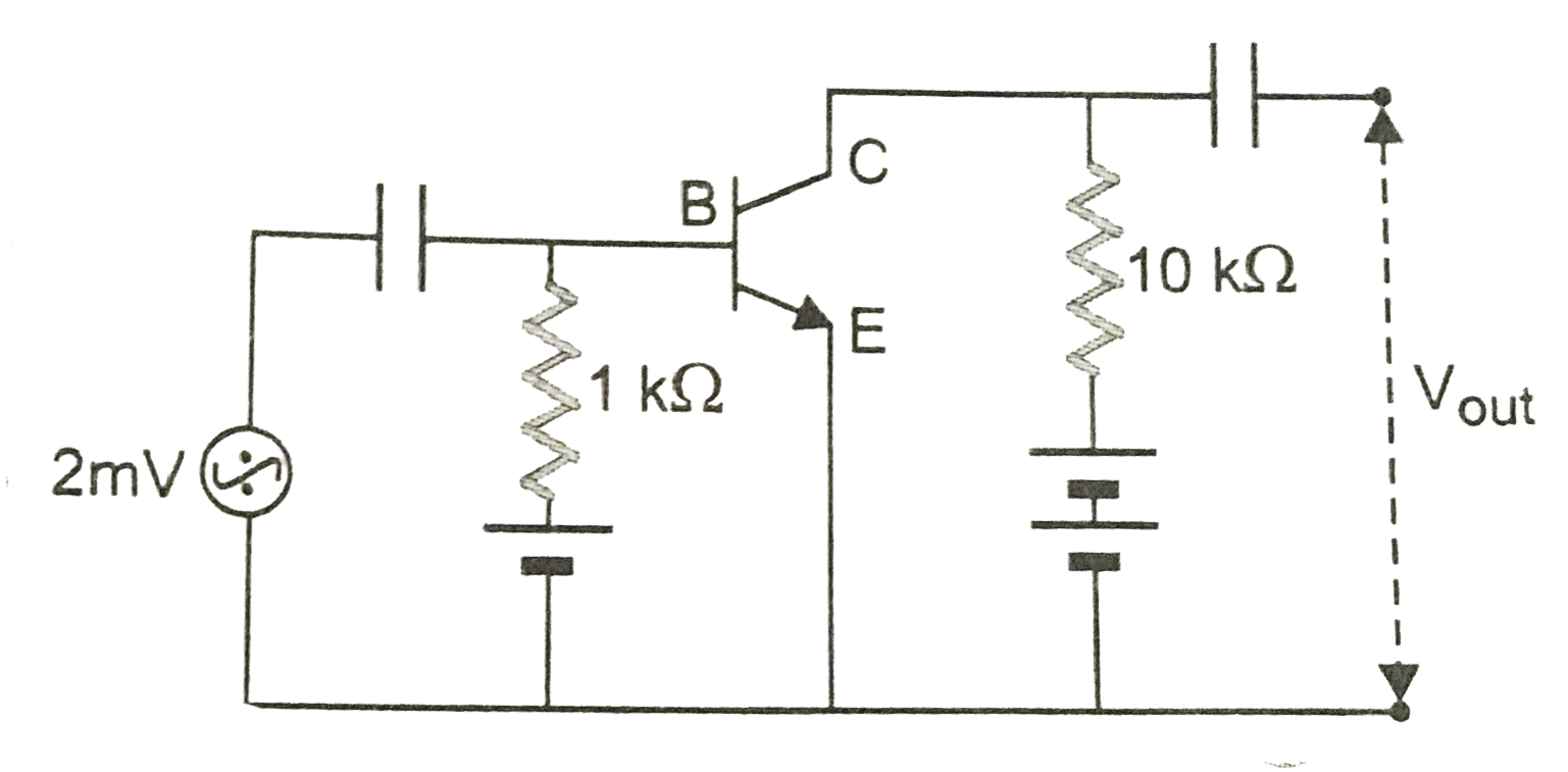
A50μAB0.5mAC2mAD2μAIn the common emitter amplifier circuit, Fig. an npn transistor with output voltage of the amplifier as 1 V, the current gain of transistor amplifier is :
 A20B25C50D75
Draw the circuit diagram for studying the characteristics of a transistor in common emitter configuration. Explain briefly and show how input and output characteristics are drawn.
View SolutionFor a transistor, α=0.99. Find the value of emitter current (in mA ) in common emitter connection for the same transistor if the value of base current is 10μA.
View SolutionDefine current amplification factor in a common emitter mode of transistor.
View SolutionExplain the input and output characteristics curves for a common emitter transistor.
View SolutionDefine the dynamic output resistance of a transistor amplifier in common - emitter configuration.
View Solution
