Discuss the working of transistor in CE configuration as a switch.
Text Solution
For the study of base biased transistor in CE configuration the circuit diagram is as shown in the figure.

Applying Kirchhoff.s rule to the input and output circuits, we have
VBB=IBR2+VBE
and VCE=VCC−ICR1
We shall take VBB as d.c. input voltage Vi and VCE as the d.c. output voltage Vo. So
Vi=IBR2+VBE
Vo=VCC−ICR1
If we study the variation of Vi versus Vo, the graph obtained is shown in figure. The graph between Vo and Vi is known as the transfer characteristics of base biased transistor. the portion of graph CD is known as cut off region, DE known as active region and portion beyond E is shown as saturation region.

(i) When Vi is less than A , the transistor is in cut off region and IC will be zero. Hence Vo=VCC
(ii) As Vi becomes greater than A, the current IC start increasing and Vo decreases asteh term ICRi increases.
(iii) With further increase in Vi,IC increases linearly, So Vo decreases linearly.
(iv) Further increase inVi,Vo decreases and never becomes zero.
From graph it is observed that transition from cut off state to activestate and from active state to saturation state are not sharply defined.
|
Similar Questions
Knowledge Check
ट्रांजिस्टर के विभिन्न विन्यासो (configurations ) का वर्णन करे ।
AInput resistance is very large while output resistance is very smallBinput resistance is very small while output resistance is very highCboth input and output resistance are very smallDboth input and output resistances are very large
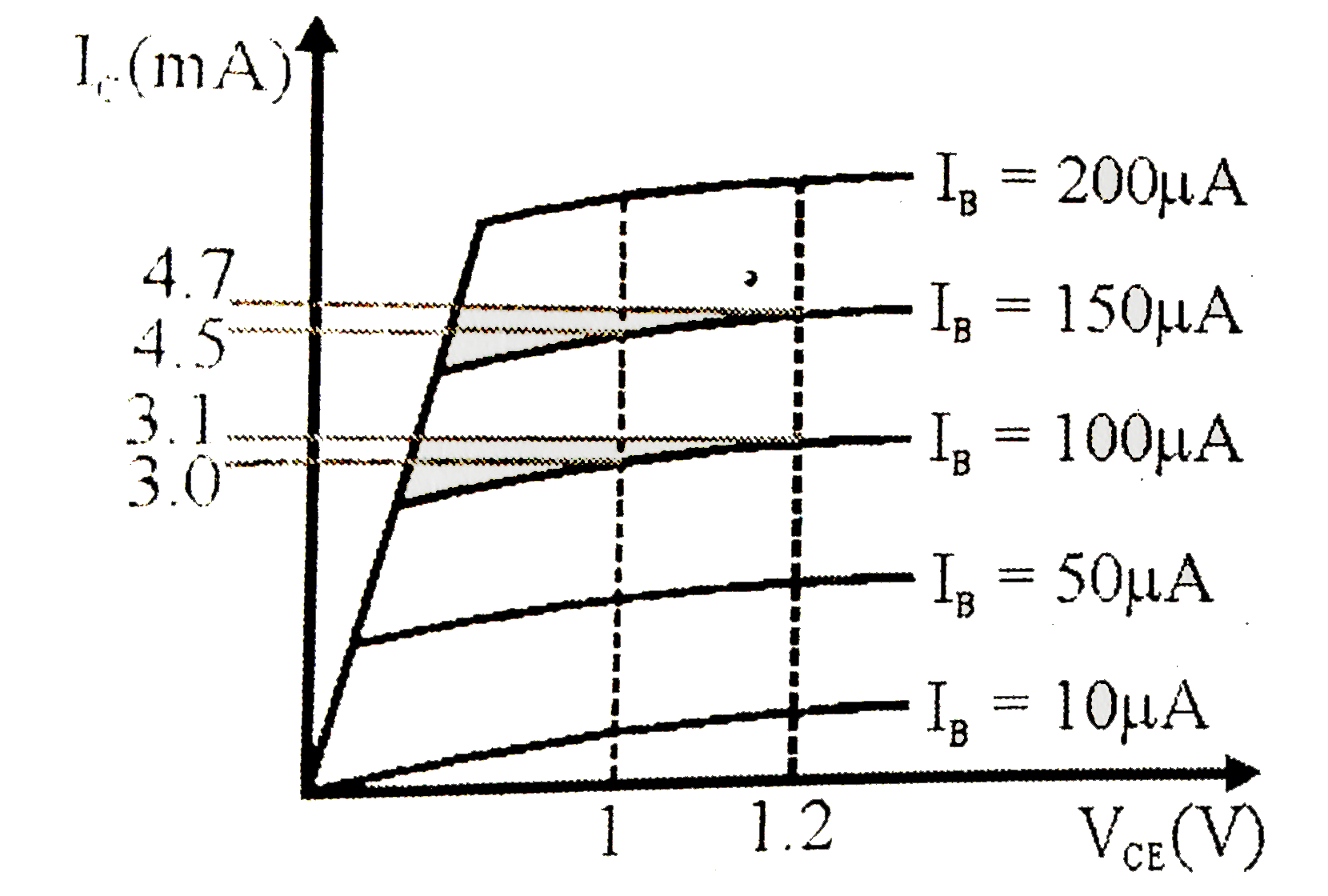
Output characteristic of n-p-n transistor in CE configuration is shown. From the characteristic curve determine the current gain at VCE=1V-A30B32C28D40The dc current gain of a transistor in CB configuration is 0.99 . Find its dc current gain in CE configuration.
A99B400C300D50
Explain the working of a transistor as a switch.
View SolutionExplain the working of a transistor as a switch.
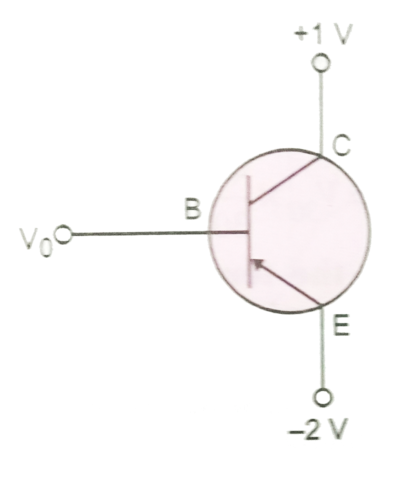
View SolutionIn Fig. is (i) the emitter, and
(ii) the collector, forward or reverse biased?

Under what condition does the transistor with CE configuration act as an amplifier?
View SolutionDraw the tramsfer characteristic curve of a base biased transistor in CE configuration. Explain clearly how the active region of the Vo versus Vi curve in a transistor is used as an amplifier.
View SolutionDraw the tramsfer characteristic curve of a base biased transistor in CE configuration. Explain clearly how the active region of the Vo versus Vi curve in a transistor is used as an amplifier.
View Solution
