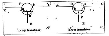
Draw the circuit symbols for p-n-p and 'n-p-n transistors.
Topper's Solved these Questions
Similar Questions
(a) Draw the circuit arrangement for studying the input and output characteristics of an n-p-n transistor in CE configuration . With the help of these characteristics define (i) input resistance , (ii) current amplification factor .
(b) Describe briefly with the help of a circuit diagram how an n-p-n transistor is used to produce self-sustained oscillations .View SolutionThe symbol of p-n-p transistor is
View Solution
Knowledge Check
- Question 1 - Select One
In an n-p-n transistor
Athe emitter has higher degree of doping compared to that of the collectorBthe collector has higher degree of doping compared to that of the emitterCboth the emitter and collector have same degree of dopingDthe base region is most heavily doped. - Question 2 - Select One
The symbol of p-n-p transistor is
A B
B C
C D
D
- Question 3 - Select One
The carriers in base region of a p-n-p transistor are
Aminority carriersBmajority carriersCboth 'a' and 'b'Delectrons
Draw a circuit diagram to show biasing of a p-n-p transistor. Explain the transistor action.
View SolutionDraw the symbol of a p-n-p transistor. Show the biasing of a p-n-p transistor and explain the transistor action.
View Solution(i) Draw a circuit diagram to study the input and output characteristics of an n-p-n transistor in its common emitter configuration. Draw the typical input and output characteristics.
(ii) Explain, with the hepl of a circuit diagram, the working of n-p-n transistor as a common emitter amplifier.View SolutionDraw a labelled circuit diagram of n - p - n germanium transistor in common emitter configuration. Explain briefly, how this transistor is used as a voltage amplifier.
View SolutionDraw the circuit diagram for studying the characteristics of a transistor in common emitter configuration. Explain briefly and show how input and output characteristics are drawn.
View Solution


