In a properly biased transistor-
Both depletion layers are equally large
Both depletion layers are equally small
Emitter base depletion layer is large but base collector depletion layer is small
Emitter base depletion layer is small but base collector depletion layer is large
The correct Answer is:D
Step by step video, text & image solution for In a properly biased transistor- by Physics experts to help you in doubts & scoring excellent marks in Class 12 exams.
Updated on:21/07/2023Topper's Solved these Questions
- SEMICONDUCTOR ELECTRONICS: MATERIALS, DEVICES AND SIMPLE CIRCUITSBOOK - AAKASH INSTITUTECHAPTER - SEMICONDUCTOR ELECTRONICS: MATERIALS, DEVICES AND SIMPLE CIRCUITSEXERCISE - Assignment (Section -B (Objective type question (one option is correct))
29 Videos
- SEMICONDUCTOR ELECTRONICS: MATERIALS, DEVICES AND SIMPLE CIRCUITSBOOK - AAKASH INSTITUTECHAPTER - SEMICONDUCTOR ELECTRONICS: MATERIALS, DEVICES AND SIMPLE CIRCUITSEXERCISE - Assignment (Section -C(Linked comprehension type question))
3 Videos
- SEMICONDUCTOR ELECTRONICS: MATERIALS, DEVICES AND SIMPLE CIRCUITSBOOK - AAKASH INSTITUTECHAPTER - SEMICONDUCTOR ELECTRONICS: MATERIALS, DEVICES AND SIMPLE CIRCUITSEXERCISE - Try yourself
20 Videos
- SEMICONDUCTOR ELECTRONICS (MATERIAL, DEVICES AND SIMPLE CIRUITS )BOOK - AAKASH INSTITUTECHAPTER - SEMICONDUCTOR ELECTRONICS (MATERIAL, DEVICES AND SIMPLE CIRUITS )EXERCISE - Assignment SECTION - D (Assertion & reason type Question)
10 Videos
- SYSTEM OF PARTICLES AND ROTATIONAL MOTIONBOOK - AAKASH INSTITUTECHAPTER - SYSTEM OF PARTICLES AND ROTATIONAL MOTIONEXERCISE - Try Yourself
63 Videos
Similar Questions
Knowledge Check
The main current, crossing the collector junction in a normally biased n-p-n transistor, is
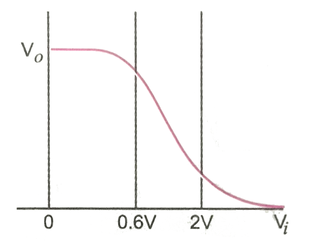
Ahole currentBdrift currentCbase currentDdiffusion currentFig.shows that transfer characteristics of a base biased CE transistor. Which of the following statements are true?
 AAt Vi=0.4V, transistor is in active stateBAt Vi=IV, it can be used as an amplifierCAt Vi=0.5V, it can be used as a switch turned offDAt Vi=2.5V, can be used as a switch turned on
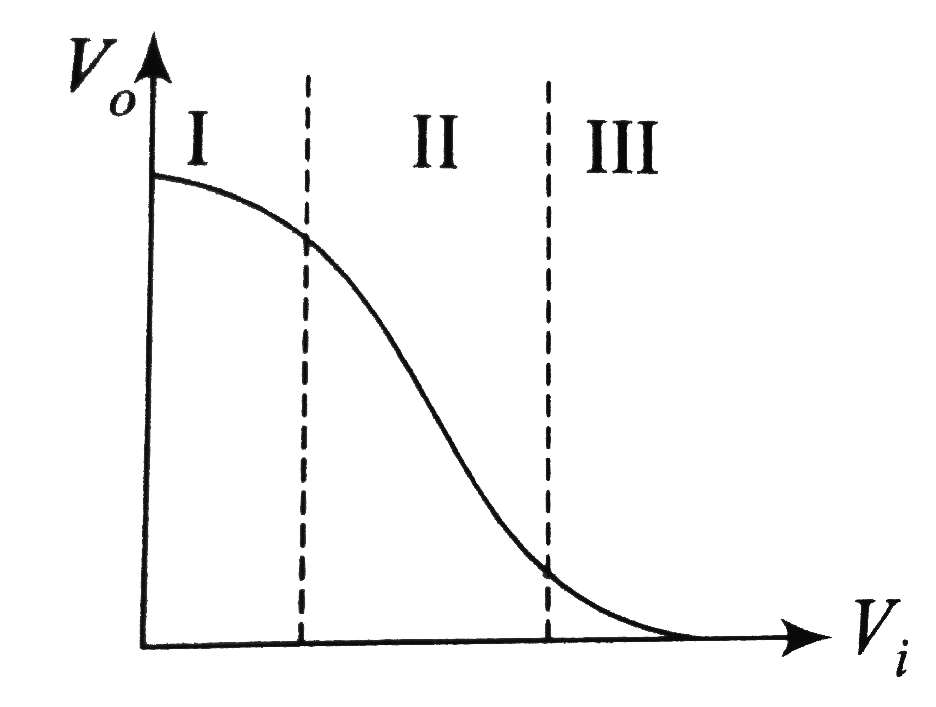
Transfer characterstics [output voltage (Vo) vs. input voltage (Vi)] for a base biased transistor in CE configuration is as shown in the figure. For using transfor as a which, it is used
 Ain region IBin region IIICboth in regios (I) and in (III)Din region II
What will happen if emitter as well as collector in a transistor are forward biased?
View SolutionDraw the tramsfer characteristic curve of a base biased transistor in CE configuration. Explain clearly how the active region of the Vo versus Vi curve in a transistor is used as an amplifier.
View SolutionDraw the transfer characteristic curve of a base biased transistor in CE configuration. Explain clearly how the active region of the Vo versus Vi curve in a transistor is used as an amplifier.
View SolutionTransistor and its properties|Transistors uses
View SolutionIn a normal operation of a transistor,
(i) base-emitter junction is forward-biased
(ii) base-collector junction is forward-biased
(iii) base-emitter junction is reverse-baised
(iv) base-collector junction is reverse-biased
View Solution
