Explain n and p-type semiconductor based on band theory. Solution in Gujrati
In extrinsic semiconductor because of the abundance of majority current carriers the minority carriers produced thermally have more chance of meeting majority carriers and thus getting destroyed and indirectly helps to reduce the intrinsic concentration of minority carriers.
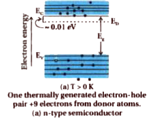
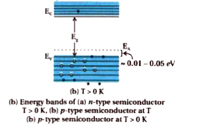
The semiconductor.s energy band structure is affected by doping. In extrinsic semiconductor, additional energy states due to donor impurities ED and acceptor impurities EA also exist.
In n-type of Si semiconductor, the donor energy level ED is slightly below the bottom EC of the conduction band and electrons from this level move into the conduction band with very small of energy.
At room temperature most of donor atoms get ionised but very few (~1012) atoms of Si get ionised so the conduction band will have most electrons coming from the donor impurities as shown in figure (a).

For p-type semiconductor the acceptor energy level EA is slightly above the top EV of the valence band. With very small supply of energy an electron from the valence band can jump to the level EA and ionise the acceptor negatively.
In other words, with very small supply of energy the hole from level EA sinks down into the valence band EV and electron comes up. This is shown in figure (b).

At room temperature, most of the acceptor atoms get ionised leaving holes in the valence band EV.
Thus, at room temperature the density of holes in the valence band is mostly due to impurity in the extrinsic semiconductor.
The above description is grossly approximate and hypothetical it helps in understanding the difference between metals, insulators and semiconductors (extrinsic and intrinsic) in a simple manner.
The energy difference between EV and EC for C (diamond) is 5.4 eV, for Si is 1.1 eV and for Ge it is 0.7 eV and Sn is also a group IV element but it is a metal because the energy gap in its case is 0 eV.
Topper's Solved these Questions
- BOOK - KUMAR PRAKASHANCHAPTER - SEMICONDUCTOR ELECTRONICS : MATERIALS, DEVICES AND SIMPLE CIRCUITS EXERCISE - Section-B : Numericals (Numerical From Textual illustrations)16videos
SEMICONDUCTOR ELECTRONICS : MATERIALS, DEVICES AND SIMPLE CIRCUITS
- BOOK - KUMAR PRAKASHANCHAPTER - SEMICONDUCTOR ELECTRONICS : MATERIALS, DEVICES AND SIMPLE CIRCUITS EXERCISE - Section-B : Numericals (Numerical From Textual Exercise)15videos
SEMICONDUCTOR ELECTRONICS : MATERIALS, DEVICES AND SIMPLE CIRCUITS
- BOOK - KUMAR PRAKASHANCHAPTER - SEMICONDUCTOR ELECTRONICS : MATERIALS, DEVICES AND SIMPLE CIRCUITS EXERCISE - Section-D : Multiple Choice Questions (MCQs) (MCQs asked in Competitive Exams)129videos
SEMICONDUCTOR ELECTRONICS : MATERIALS, DEVICES AND SIMPLE CIRCUITS
- BOOK - KUMAR PRAKASHANCHAPTER - SAMPLE QUESTION PAPER EXERCISE - PART-B SECTION-C5videos
SAMPLE QUESTION PAPER
- BOOK - KUMAR PRAKASHANCHAPTER - WAVE OPTICSEXERCISE - SECTION-D (MULTIPLCE CHOICE QUESTIONS (MCQS)) (MCQS FROM DARPAN BASED ON TEXTBOOK)239videos
WAVE OPTICS
Similar Questions
C, Si and Ge have same lattice structure. Why is C insulator while Si and Ge intrinsic semiconductors?
06:16View SolutionIn an n type silicon, which of the following statements is true:
04:44View SolutionAt absolute zero temperature Si acts as ……..
05:24View SolutionTwo charges –q and +q are located at points (0, 0, –a) and (0, 0, a), respectively.
(a) What is the electrostatic potential at the points (0, 0, z) and (x, y, 0) ?
(b) Obtain the dependence of potential on the distance r of a point from the origin when r/a>>1 .
(c) How much work is done in moving a small test charge from the point (5,0,0) to (–7,0,0) along the x-axis? Does the answer change if the path of the test charge between the same points is not along the x-axis?12:42View SolutionAccording to particle theory of light what is the velocity of light in a dense medium, compared to that in rare medium ?
05:20View SolutionENERGY BAND DIAGRAMS OF P-TYPE AND N-TYPE SEMICONDUCTORS
06:31View Solutionनैज अर्द्धचालक, n - प्रकार के अर्द्धचालक तथा p - प्रकार के अर्द्धचालक के ऊर्जा बैण्ड चित्र दर्शाइये।
06:43View SolutionExplain the electrical conductivity of a semiconductor with the help of band theory.
02:42View SolutionExplain how an intrinsic semiconductor can be converted into an n-type semiconductor and a p-type semiconductors. Draw the energy band diagrams of n-type and p-type semicon ductors.
04:30View Solutionp-टाइप तथा n-टाइप के अर्धचालक क्या है ? समझाए ।
11:17View SolutionP- प्रकार के अर्द्धचालक को ऊर्जा बैण्ड के पदों में समझाइए।
07:15View Solutionn- प्रकार के अर्द्धचालक को ऊर्जा बैण्ड के पदों में समझाइए।
06:45View Solutionऊर्जा बैंड आरेख के आधार पर n-प्रकार और p-प्रकर के अर्धचालकों में अंतर् लिखिए |
View Solutionबैण्ड सिद्धांत के आधार पर चालक, अर्धचालक और कुचालक को समझाइए तथा ऊर्जा आरेख बनाइए।
33:49View Solutionऊर्जा बैंड सिद्धांत के आधार पर चालकों, अर्धचालकों तथा कुचालकों में विभेदन स्पष्ट कीजिये| नैज अर्धचालकों में धारा चालन की प्रक्रिया समझाइये|
05:27View Solution

