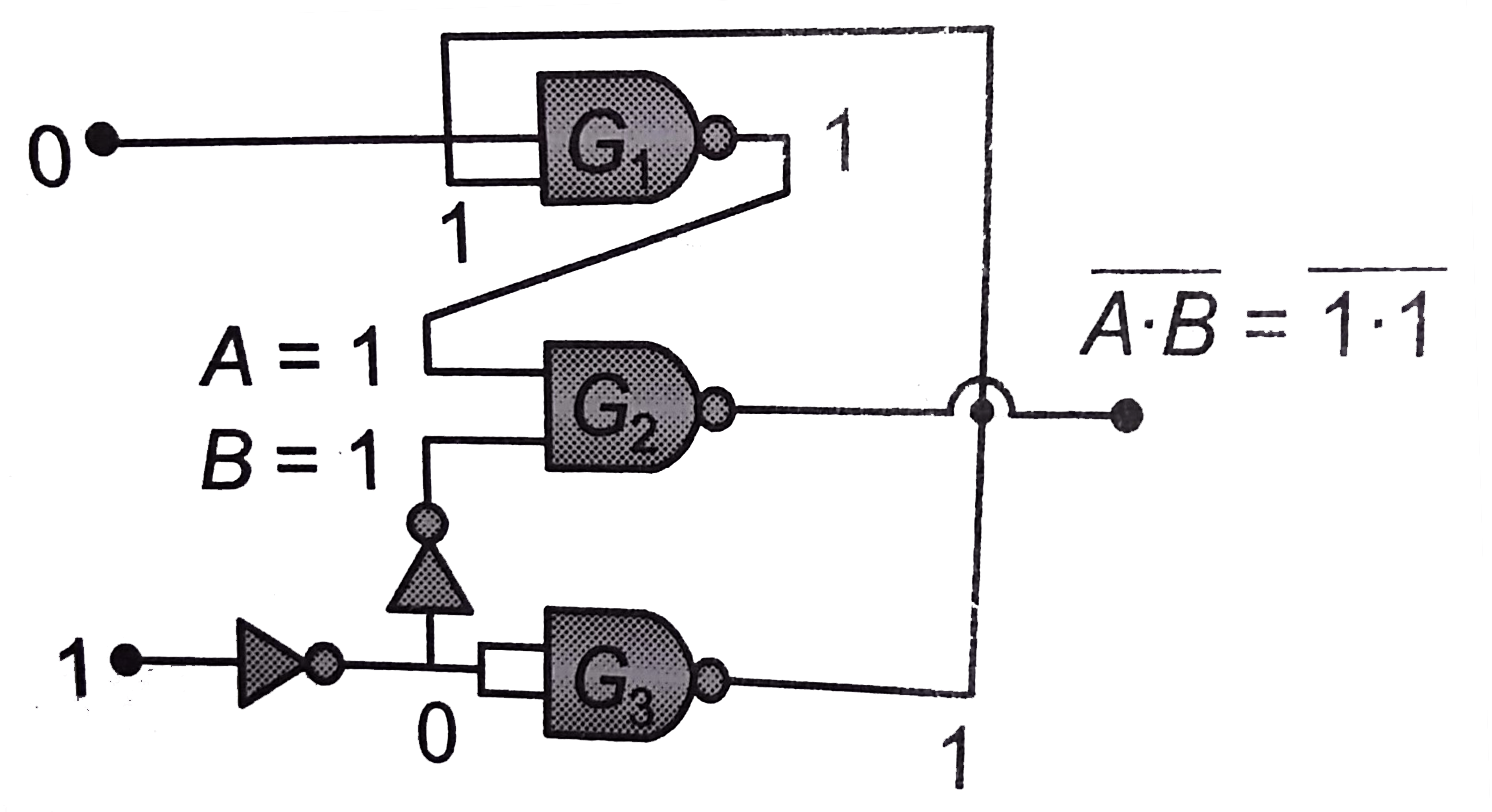
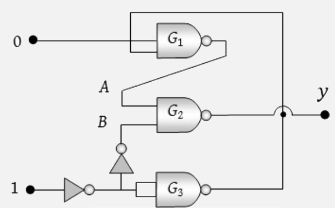
In circuit in the following figure the value of Y is
A
0
B
1
C
Fluctuates between 0 and 1
D
Indeterminate as the circuit can't be realised
Text Solution
The correct Answer is:A
Lower NOT gate inverts input to zero. NOT gate from NAND gate inverts this output to 1 upper NAND gate converts this input 1 and input 0 to 1.
Thus A=1 and B=1 become inputs of NAND gate giving final outputs as zero. Choice (a) is correct.
|
Topper's Solved these Questions
- SEMICONDUCTOR ELECTRONICSBOOK - A2ZCHAPTER - SEMICONDUCTOR ELECTRONICSEXERCISE - Problems Based On Mixed Concepts
32 Videos
- SEMICONDUCTOR ELECTRONICSBOOK - A2ZCHAPTER - SEMICONDUCTOR ELECTRONICSEXERCISE - Section B - Assertion Reasoning
22 Videos
- SEMICONDUCTOR ELECTRONICSBOOK - A2ZCHAPTER - SEMICONDUCTOR ELECTRONICSEXERCISE - Junction Transistor
47 Videos
- NUCLEAR PHYSICSBOOK - A2ZCHAPTER - NUCLEAR PHYSICSEXERCISE - Section D - Chapter End Test
29 Videos
- SOURCE AND EFFECT OF MAGNETIC FIELDBOOK - A2ZCHAPTER - SOURCE AND EFFECT OF MAGNETIC FIELDEXERCISE - Section D - Chapter End Test
30 Videos
Similar Questions
Knowledge Check
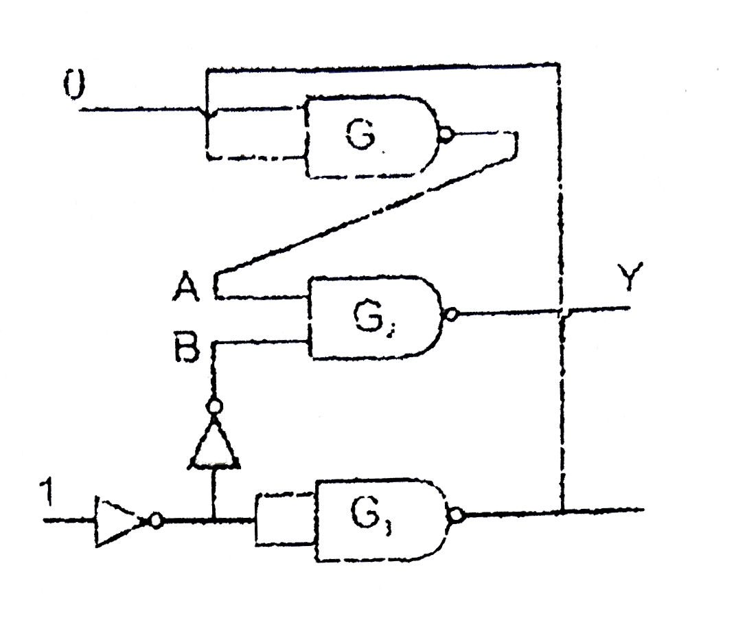
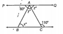
In circuit in following figure the value of Y is-AZeroB1Cfluctuates between 0 and 1Dindeterminate as the circuit cannot be realizedIn the following figure, find the value of y :
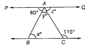 A70∘B60∘C50∘D80∘
For the circuit shown in the following figure, the
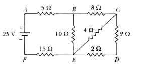 APotential difference between points B and E is 5 VBPotential difference between points A and B is 10 VCCurrent in the 4Ω resistor is 0.25ADCurrent in the 4Ω resistor is 0.5 A
In the circuit shown in the following figure, the value of Y is
View SolutionIn the following figure, find the value of y.
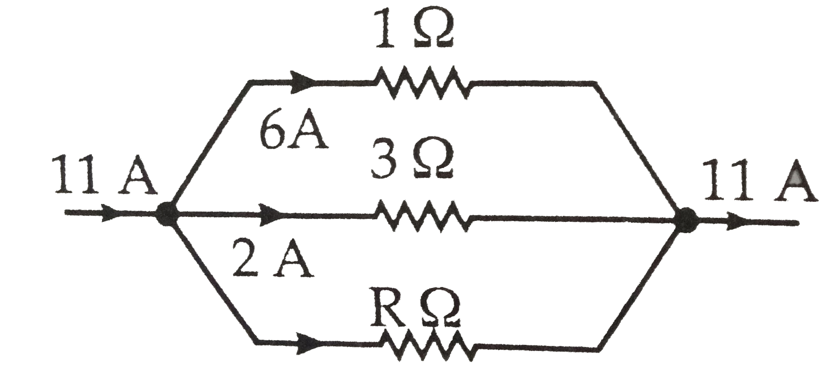
View SolutionIn the circuit shown in figure, the value of R is
View SolutionIn each of the following figures, find the values of x and y

View SolutionIn each of the following figures, find the values of x and y

View Solution
