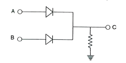
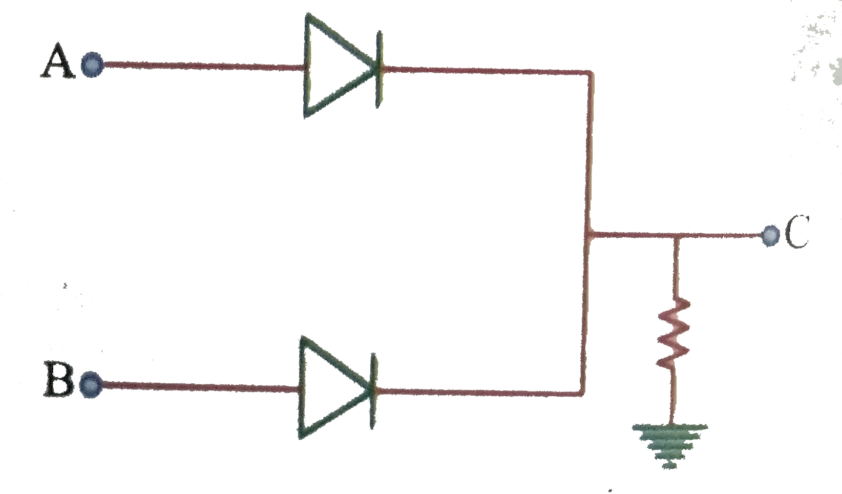
In the circuit below , A and B represent two inputs and C represents the output . The circuit represents
 Solution in Kannada
OR gate
NOR gate
AND gate
NAND gate.
The correct Answer is:A
It is circuit diagram for OR gate because when either A or B is high the output at C is high
=W(1+Y)+XW+XY
=W.1+XW+XY (∵1+Y=1)
=W(1+W)+XY
=W+XY (∵1+X=1)
Topper's Solved these Questions
- BOOK - MODERN PUBLICATIONCHAPTER - SOLIDS & SEMICONDUCTOR DEVICESEXERCISE - Multiple Choice Questions - LEVEL -I (ASSERTION)5videos
SOLIDS & SEMICONDUCTOR DEVICES
- BOOK - MODERN PUBLICATIONCHAPTER - SOLIDS & SEMICONDUCTOR DEVICESEXERCISE - Multiple Choice Questions - LEVEL -I (PARAGRAPH)6videos
SOLIDS & SEMICONDUCTOR DEVICES
- BOOK - MODERN PUBLICATIONCHAPTER - ROTATIONAL MOTIONEXERCISE - RCQ8videos
ROTATIONAL MOTION
- BOOK - MODERN PUBLICATIONCHAPTER - TRANSFERENCE OF HEAT EXERCISE - Recent Competitive Questions4videos
TRANSFERENCE OF HEAT
Similar Questions
Statement I : In N - type semiconductor , the free electron concentration approximately equals the density of donor atoms .
Statement II : In a forward biased P - N - region is proportional to the change Q of the injected minority carrier holes.02:19View SolutionIn a triode value for a grid voltage Vg=−1.2V , the phase current Ip and plate voltage Vp are given Ip=(−5+0.1V0),Ip in mAandVp in volt . When grid voltage is changed to - 3.2 V at constant plate voltage of 150 V , a plate current of 5 mA is observed , then
Plate resistance Rp is03:29View SolutionThe moment of inertia of a circular disc of radius 2 m and mass 1 kg about an axis passing through the centre of mass but perpendicular to the plane of the disc is 2 kg m2. Its moment of inertia about an axis parallel to this axis but passing through the edge of the disc is :
 03:33View Solution
Two slabs are of the thicknesses d1 and d2. Their thermal conductivities are K1 and K2 respectively They are in series. The free ends of the combination of these two slabs are kept at temperatures θ1 and θ2. Assume θ1>θ2. The temperature θ of their common junction is
04:38View SolutionThe diagram of a logic circuit is given below. The output F of the circuit is represented by
02:49View SolutionIn the circuit below, A and B represents two inputs and C represents the output, the circuit represents.
 .02:49View Solution
In the circuit below, A and B represents two inputs and C represents the output . The circuit represents
 05:20View Solution
In the circuit below, A and B represent two inputs and C represents the output. The circuit represents
04:25View SolutionThe diagram of a logic circuit is given below . The output F of the circuit is represented by :
01:50View SolutionThe diagram of a logic circuit is given below . The output F of the circuit is represented by :
View SolutionIn the circuit given below, A and B represent the inputs of the two input gates and C represents one output. Displays the circuit.
03:40View SolutionIn the circuit below, A and B represent two inputs and C represents one output. Circuit displays
02:17View SolutionIn the circuit below, A and B represents two inputs and C represents the output, the circuit represents.
 .View Solution
In the circuit below, A and B represent two inputs and C represents the output. The circuit represents
View SolutionIn the circuit below, A and B represents two inputs and C represents the output . The circuit represents
03:31View Solution
