In the circuit shown in the figure, there are two parallel plate capacitors each of capacitance C. The switch S1 is pressed first to fully charge the capacitor C1 and then released. The switch S2 is then pressed to charge the capacitor C2. After some time, S2 is released and then S3 is pressed. After some time
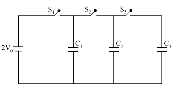
the charge on the upper plate of C1is2CV0
the charge on the upper plate of C1isCV0
the charge on the upper plate of C2 is 0
the charge on the upper plate of C2is−CV0
After switch S1 is closed, C1 is charged by 2CV0, when switch S2 is closed C1 and C2 both have plate charge CV0. When S3 is closed, then upper plate of C2 becomes charged by −CV0 and lower plate by +CV0
Similar Questions
In the R-C circuit shown in the figure the total of 3.6×10⁻³J is dissipated in the 10 ohms resistor when the switch S is closed. The initial charge on the capacitor is
 View Solution
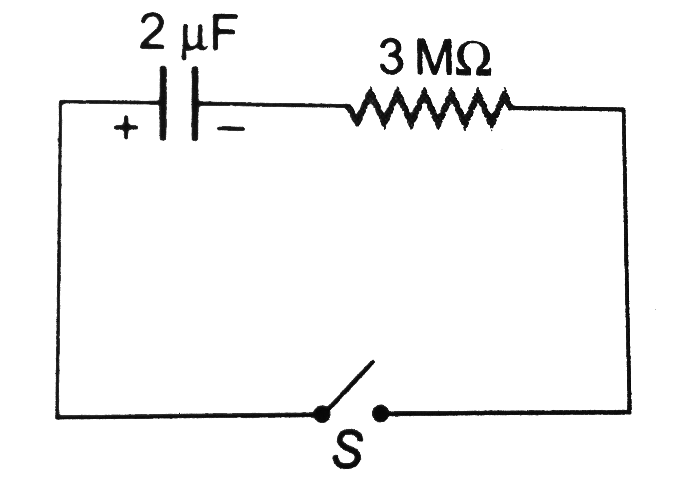
In the circuit shown in figure, the capacitor is charged with a cell of 5V.If the switch is closed at t=0, then at t=12s, charge on the capacitor is
 View Solution
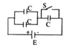
In the circuit shown, each capacitor has a capacitance C. The emf of the cell is E. If the switch S is closed
 View Solution
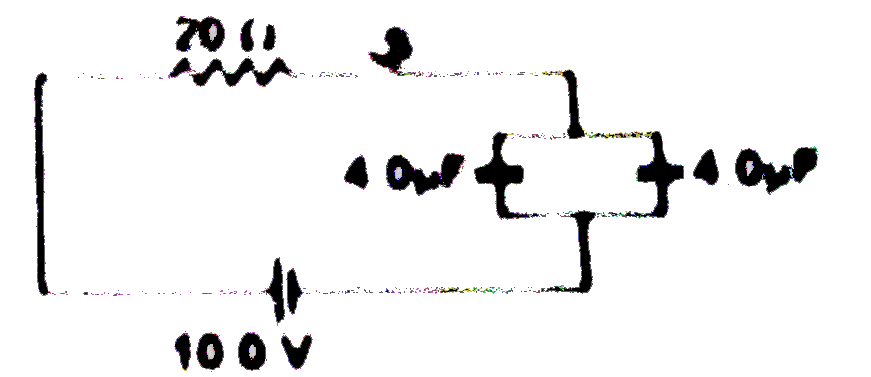
The charge on each of the capacitors 0.16 ms after the switch S is closed in figure is :
 View Solution
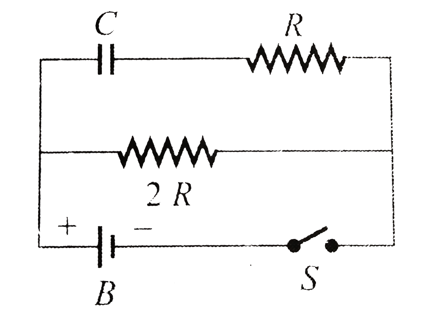
In the circuit shown in fig, if the switch S is closed at t=0 , the capacitor charges with a time constant
 View Solution
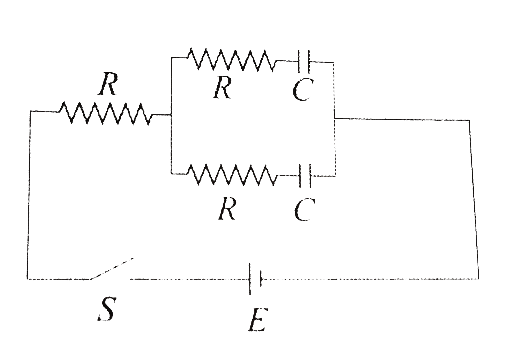
The switch S in the circuit diagram is closed at t = 0. The charge on capacitors at any time is
 View Solution
The time constant, for charging of capacitor C, when switch S is closed as shown in the figure , is
_PHY_E01_020_Q01.png) View Solution
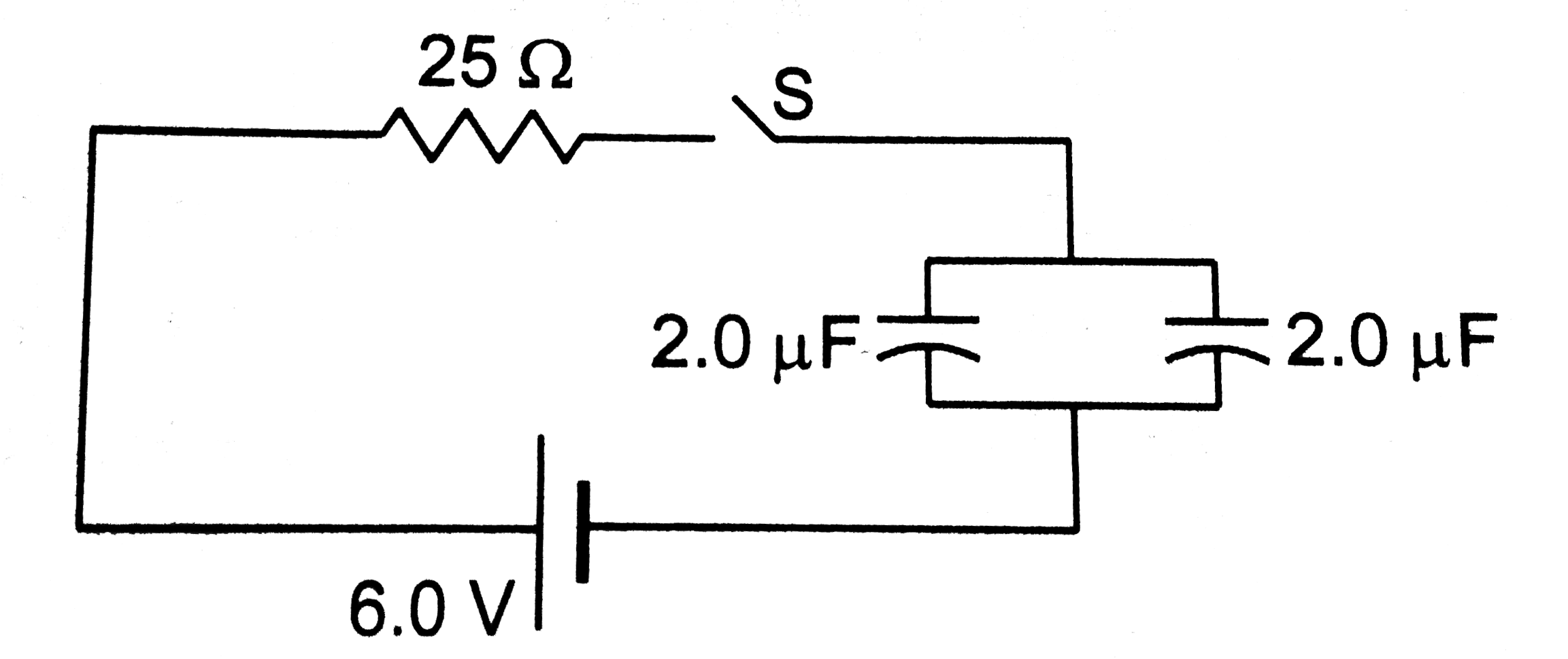
View SolutionFind the charge on each of the capacitor 0.20ms after the switch S is closed in Figure.
 View Solution
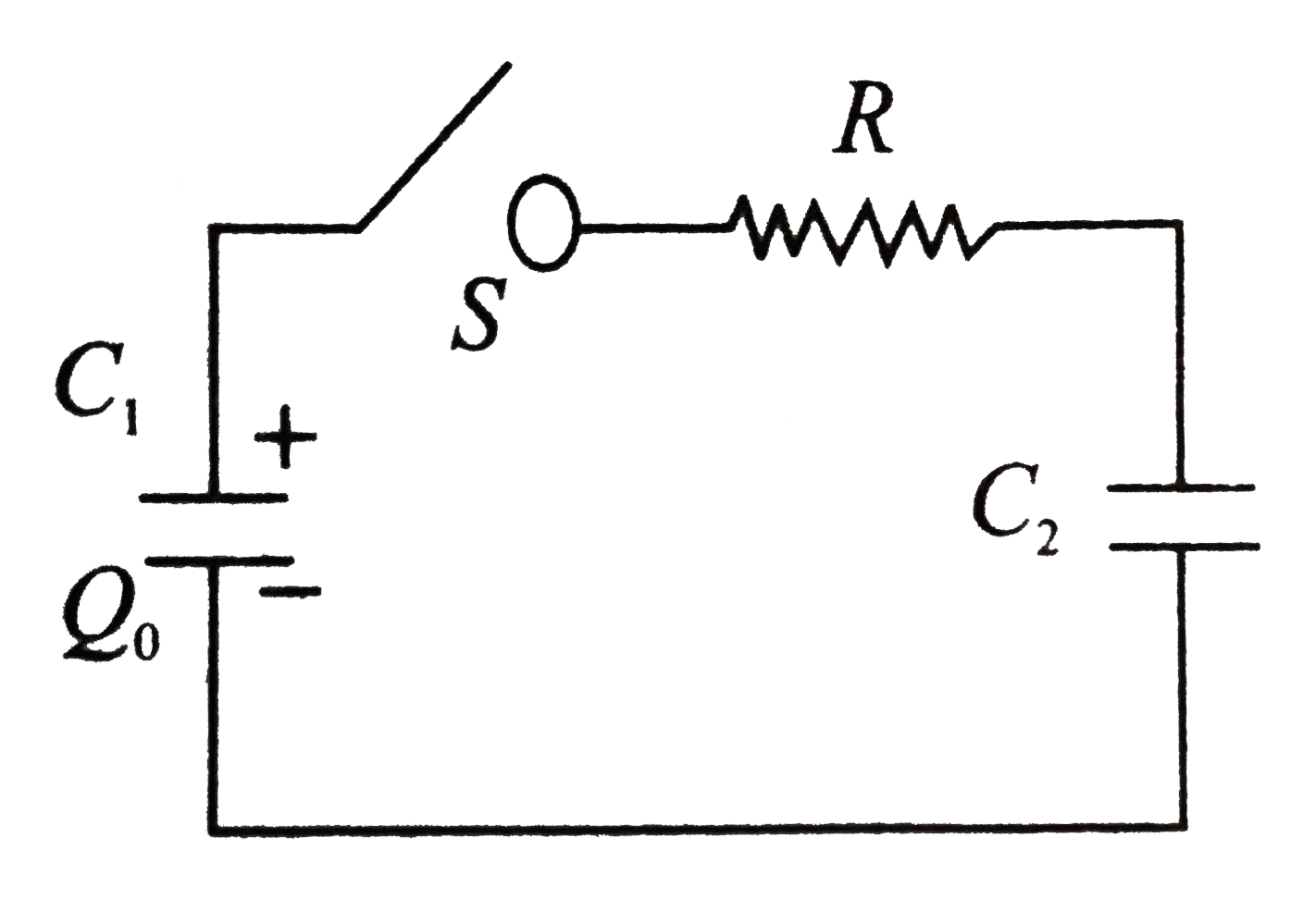
In the circuit shown, the capacitor C1 is initially charged with charge q0. The switch S is closed at time t = 0 . The charge on C2 after time t is
 View Solution
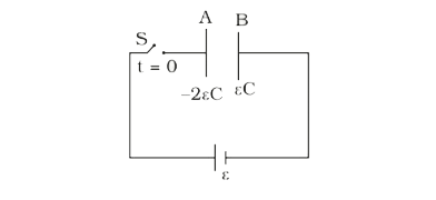
A parallel pate capacitor of capacitance ‘C’ has charge on its plates initially as shown in the figure. Now at the switch ‘S’ is closed. Select the correct alternative (s) for this circuit diagram.
 View Solution
