Complete Solutions to Assignment (Section -A (Objective Type question (One option is correct)) of chapter SEMICONDUCTOR ELECTRONICS: MATERIALS, DEVICES AND SIMPLE CIRCUITS of Class 12 book with complete answers and questions
| Class 12 | PHYSICS |
| Chapter | SEMICONDUCTOR ELECTRONICS: MATERIALS, DEVICES AND SIMPLE CIRCUITS |
| AAKASH INSTITUTE | Assignment (Section -A (Objective Type question (One option is correct)) |
| Number Of Questions | 50 |
| Academic Year | 2023-24 |
Silicon is a semiconductor. If a small amount of As is added to it, then its electrical conductivity
View SolutionThe mobility of free electrons is greater then that of free holes because
View SolutionCarbon , silicon and germanium have four valence electrons each . At room temperature which one of the following statements is most appropriate ?
View SolutionWhich circuit will not show current in ammeter ?
View SolutionA p-n photodiode is made of a material with a band gap of 2 e V. The minimum frequency of the radiation that can be absorbed by the material is nearly
(hc= 1240 eV nm)
View SolutionZener breakdown takes place if
View SolutionIn the depletion region of an unbiased p-n junction diode there are
View SolutionFunction of rectifier is
View SolutionIn a p–n junction photo cell, the value of the photo electromotive force produced by monochromatic light is proportional to: -
View SolutionSerious draw back of the semiconductor device is
View SolutionThe reason of current flow in `P-N` junction forward biase is
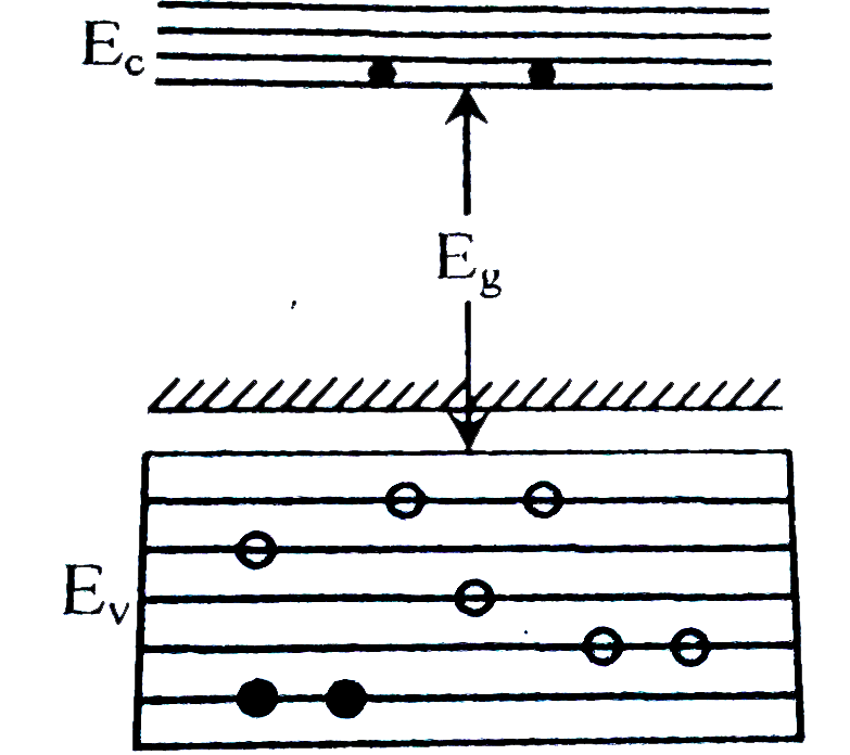
View SolutionIn the energy band diagram of a material shown below, the open circles and filled circles denote holes and electrons respectively. The material is:-
View SolutionAn oscillator is nothing but an amplifier with
View SolutionWhen a n-p-n transistor is used as an amplifier, then
View SolutionIf `l_(1),l_(2),l_(3)` are the lengths of the emitter, base and collector of a transistor then
View SolutionA common emitter amplifier gives an output of 3 V for an input of 0.01 V. If `beta` of the resistance is 100 and the input resistance is `1 kOmega`. then the collector resistance is
View SolutionIn a common base amplifier the phase difference the input signal voltage and the output voltage is
View SolutionIn a common emitter amplifier the input signal is applied across
View SolutionThe concentration of impurities in a transistor is
View SolutionIn a transistor, the collector current is always · less then the emitter current because -
View SolutionThe minimum potential difference between the base and emitter required to switch a silicon transistor ON is approximately?
View SolutionWhich of the following represents NAND gate ?
View SolutionThe circuit is equivalent to

View Solution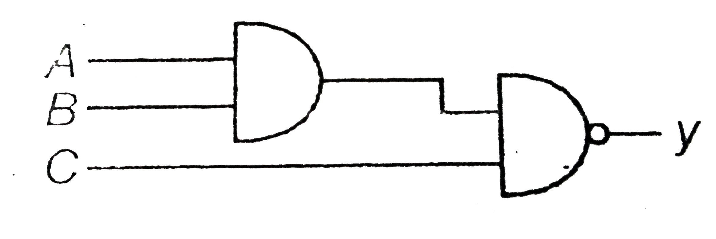
The output y, when all three inputs are first high and then low, will respectively be
View SolutionA silicon specimen is made into a `P`-type semiconductor by dopping, on an average, one helium atoms per `5xx10^(7)` silicon atoms. If the number density of atoms in the silicon specimen is `5xx10^(28) at om//m^(3)` then the number of acceptor atoms in silicon per cubic centimeter will be
View SolutionConsider the junction diode is ideal. The value of current through the resistance of `300 Omega` is

View SolutionNegative feedback
View SolutionThe current obtained from a simple filterless rectifier is
View SolutionIn a p-n junction depletion region has a thickness of the order of
View SolutionIn a properly biased transistor-
View SolutionIn an n-p-n transistor, the collector current is 10 mA. If 90% of the electrons emitted reach the collector, then the emitter current will be
View SolutionApplication of forward bias to p-n junction
View SolutionIntrinsic semiconductor at absolute zero temperature is a
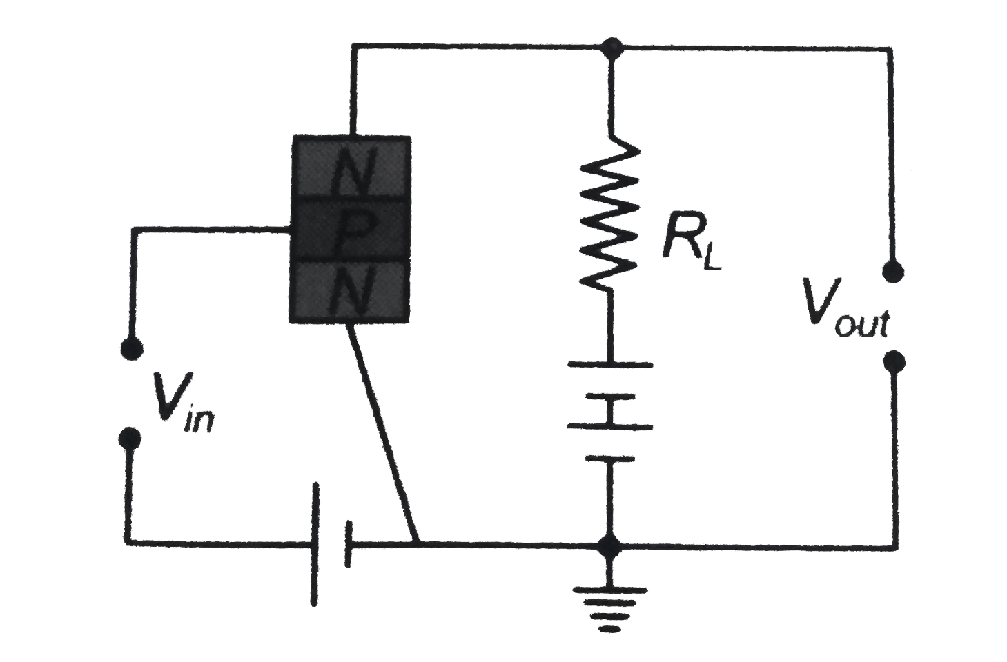
View SolutionAn `NPN`-transistor circuit is arranged as shown in figure. It is
View Solution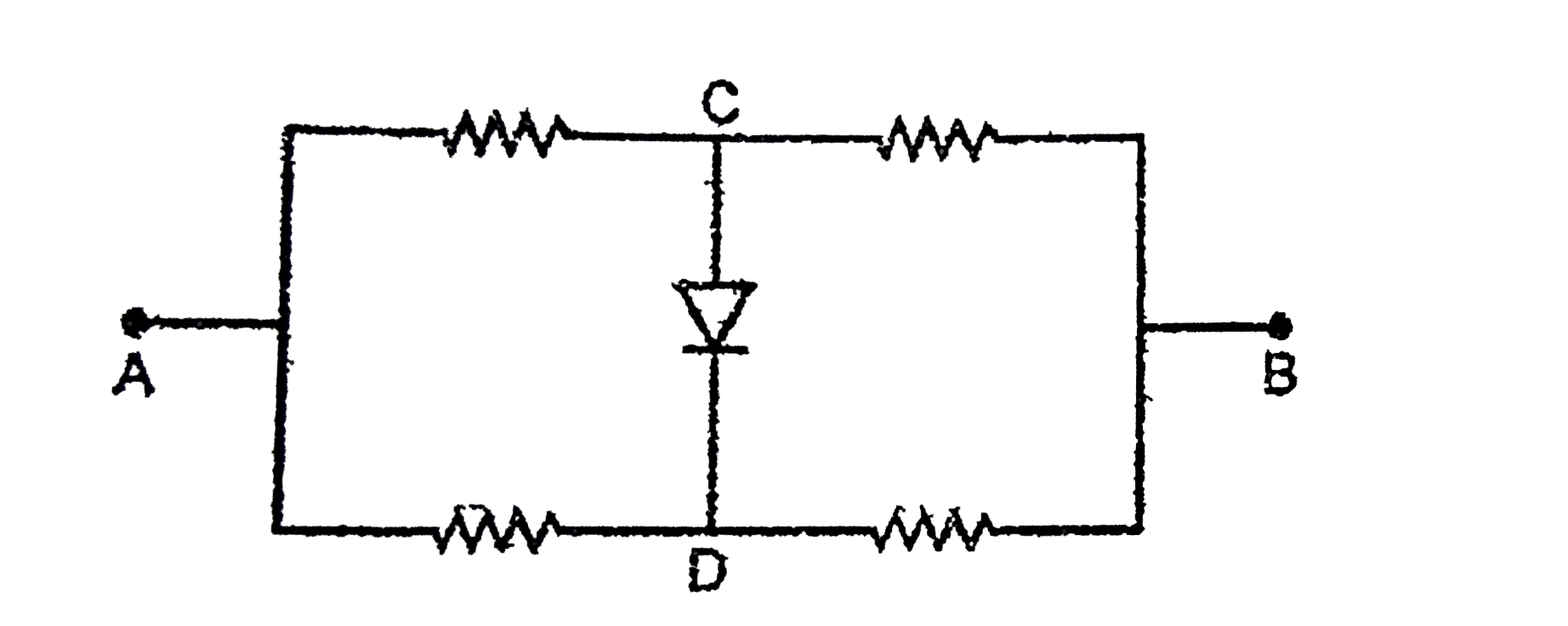
Four equal resistors, each of resistance 10 ohm are connected as shown in the adjoining circuit diagram. Then the equivalent resistance between points A and B is-
View SolutionIn a semiconducting material the mobilities of electrons and holes are `mu_(e)` and `mu_(h)` respectively. Which of the following is true?
View SolutionWhich of the following gate is called universal gate
View SolutionA full wave rectifier circuit along with the input and output are shown in Fig. the concentrations from the diode I is (are)
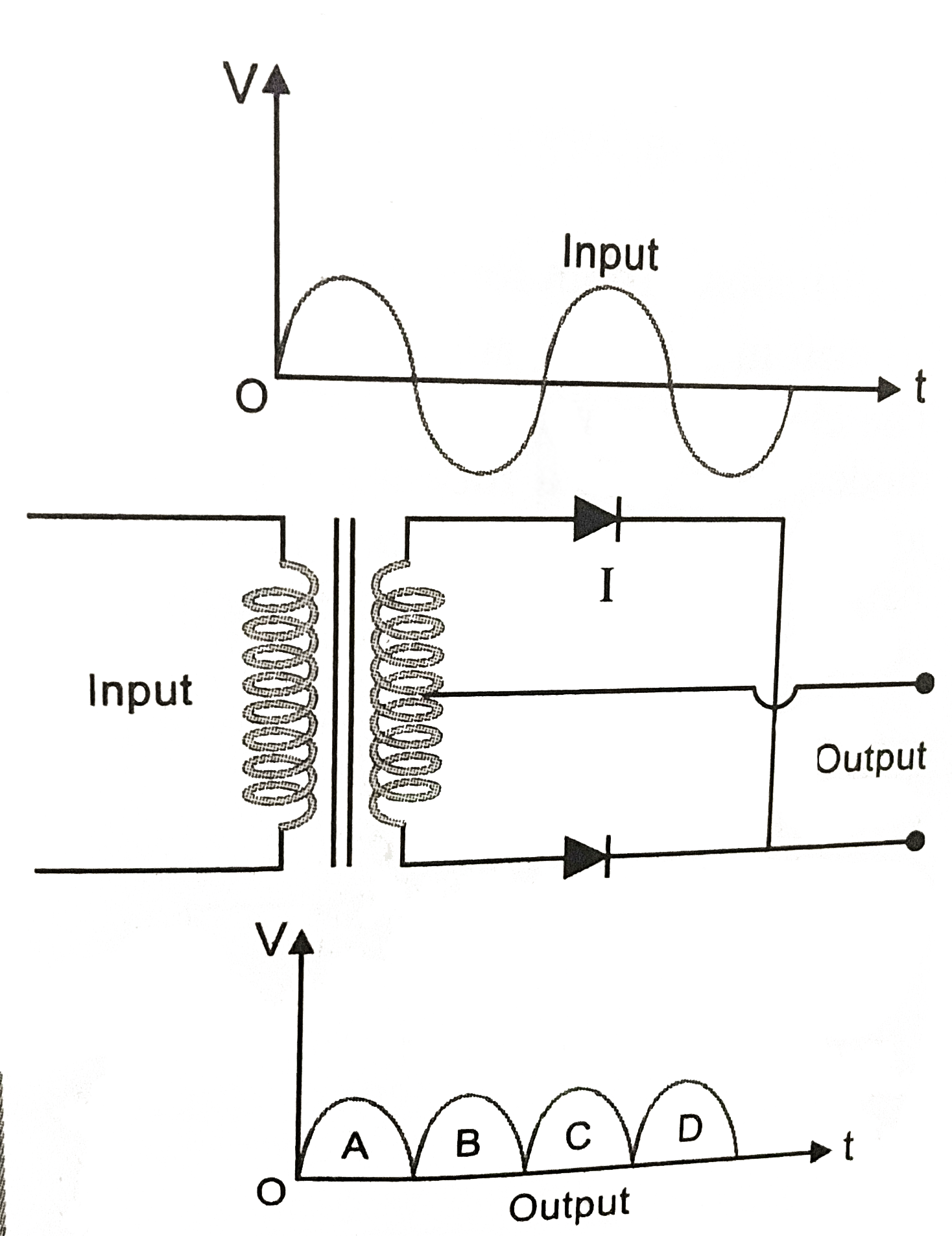
View SolutionIn a `p-n` junction diode having depletion layer of thickness `10^(-6)m`, the potential across it is `0.1V`. The electric field produced is
View SolutionWhat is the voltage gain in a common emitter amplifier, where output resistance is `3 Omega` and load resistance is `24 Omega (beta=0.6)` ?
View SolutionBarrier potential of a p-n junction diode does not depend on -
View SolutionThe following truth table corresponds to the logic gate

View SolutionWhich of the following is not equal to 1 in Boolean algebra ?
View SolutionPotential barrier developed in a junction diode opposes the flow of
View SolutionWhich of the following diodes is used in unbiased condition ?
View SolutionWhich of the following materials can be used for making solar cell ?
View SolutionIf a full wave rectifier circuit is operating from `50 Hz` mains, the fundamental frequency in the ripple frequency will be
View SolutionA transistor cannot be used as an
View SolutionThe P-N junction is-
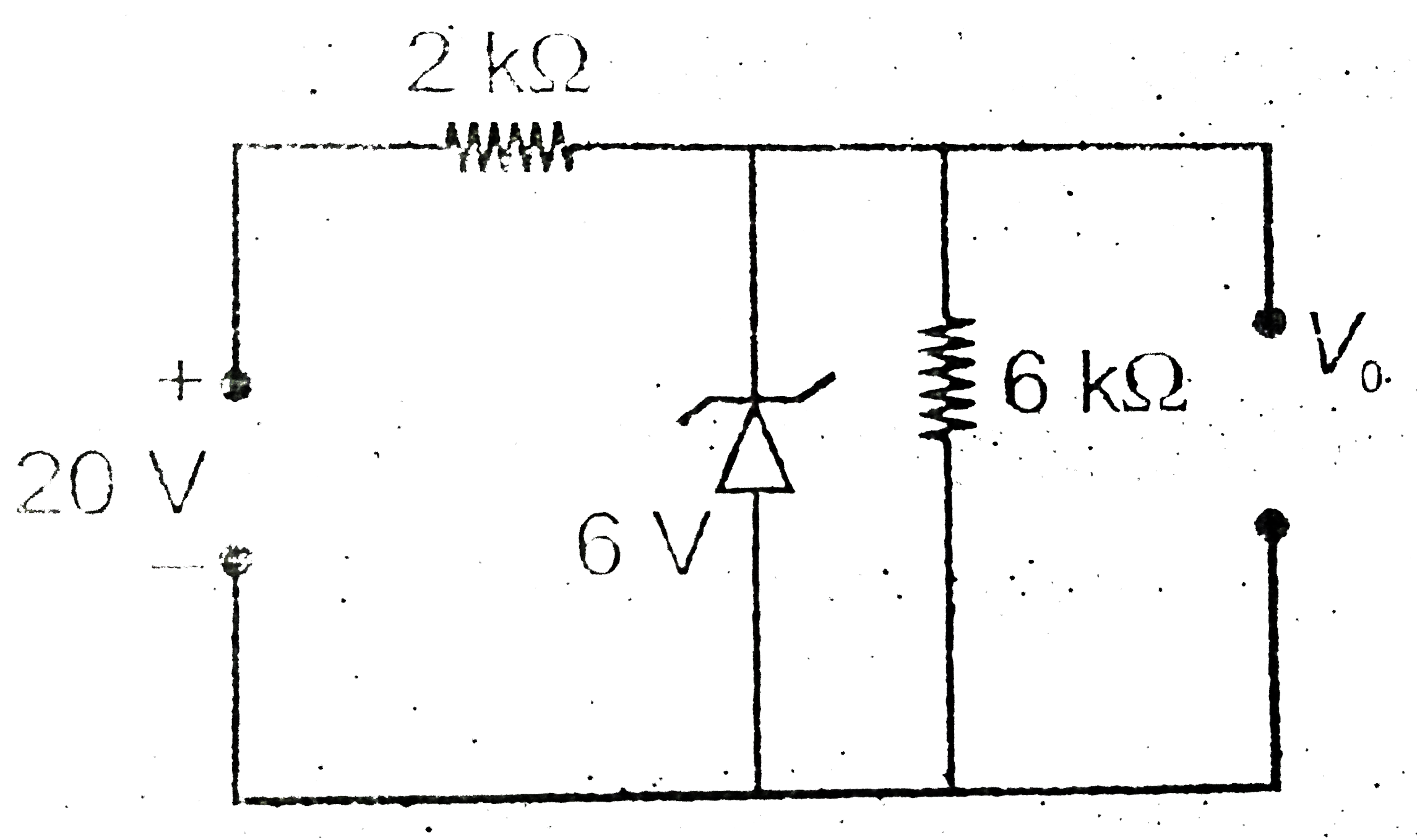
View SolutionWhat is the value of output voltage `V_(0)` in the circuit shown in the figure ?
View Solution
Assignment (Section -A (Objective Type question (One option is correct)) questions and complete solutions for chapter SEMICONDUCTOR ELECTRONICS: MATERIALS, DEVICES AND SIMPLE CIRCUITS of AAKASH INSTITUTE ENGLISH of Class 12