Complete Solutions to NCERT FILE SOLVED (TEXT BOOK EXERCISES ) of chapter SEMICONDUCTOR ELECTRONICS METERIALS DEVICES AND SIMPLE CIRCUITS of Class 12 book with complete answers and questions
| Class 12 | PHYSICS |
| Chapter | SEMICONDUCTOR ELECTRONICS METERIALS DEVICES AND SIMPLE CIRCUITS |
| MODERN PUBLICATION | NCERT FILE SOLVED (TEXT BOOK EXERCISES ) |
| Number Of Questions | 30 |
| Academic Year | 2023-24 |
In an n type silicon which of the following statement is true
(a) electrons are majortiy carriers and trivalent atoms are the dopants
(b) electrons are minority carriers and pentavalent atoms are the dopants
(c ) hoes are minority carriers and pentavalent atoms are the dopants
(d) holes are majority carriers and trivalen atoms are the dopant
View SolutionWhich of the statements given in above example is true for p - type semiconductors ?
View SolutionCarbon silicon and germanium have four valence electrons each these are characterised by valence and conduction bands separated by energy band gap respectively equal to which of the following statement is true
(a) `(E_(g))_(Si)lt(E_(g))_(Ge)lt(E_(g))_(c )`
(b)`(E_(g))_(c )lt(E_(g))_(Gelt(E_(g))_(Si)`
(c )`(E_(g))_(c )gt(E_(g))_(Si)gt(E_(g))_(Ge)`
`(d)(E_(g))_(c )=(E_(g))_(si)=(E_(g))_(Ge)`
View SolutionIn an unblased p-n junction, holes diffuse from the p - region to n- region because
View SolutionWhen a forward bias is applied to a p -n junction. It
View SolutionFor transistor action which of the following statement are correct
(a) base emitter and collector regions should have smilar size and doping concentrations
(b) the base region must be very thin and lightly doped
(c ) the emitter junction is forward biased and collector junctions is reverse biased
(d)both the emitter junction as well as the collector junction are forward biased
View SolutionFor transistor amplifier the voltage gain
(a) remains constant for all frequencies
(b) is high at high and low frequencies
(c ) is low at high and low frequencies and constant in the middle frequency range
(d) none of these
View SolutionIn half - wave rectification, what is the output frequency, if the
input frequency is 50 Hz ? What is the output frequency of a full - wave rectifier
for the same input frequency ?
View SolutionFor a CE -transistor amplifier the audio signal voltage across the collector resistance of 2 k`Omega `is 2V. Given the current amplification factor of the transistor is 100 find the input signal voltage and base current if the base resistance is 1 k `Omega`.
View SolutionTwo amplifiers are connected one after the other in series (cascaded). The first amplifier has a voltage gain of 10 and the second has a voltage gain of 20 . If the input signal is 0.01 V , calcualte the output AC signal .
View SolutionA p-n photodiode is fabricated from a semiconductor with band gap of 2.8 eV can it detect a wavelength of 6000 nm
View SolutionThe number of silicon atoms per `m^(3) is 5xx10^(28)`. This is doped simultaneously with `5xx10^(22)` atoms per `m^(3)` of Arsenic and `5xx10^(20) per m^(3)` atoms of indium. Calculate the number of electrons and holes. Given that `n_(i)=1.5xx10^(16)m^(-3)`. Is the material n-type or p-type?
View SolutionIn an intrinsic semiconductor, the energy gap `E_(g)` of an intrinsic semiconductor is 1.2 eV. Its hole mobility is very much smaller than electron mobility and is indepndent of temperature. What is the ratio between conductivity at 600K and at 300K? Assume that the temperature dependence of intrinsic concentraction `n_(i)` is expressed as,
`n_(i)=n_(o)e^(-E_(g)^(')//k_B)T`, where `n_(o)` is constant and `E_(g)^(')` is an energy equal to `E_(g)//2`,
`k_(B)=8.62xx10^(-6)eVK^(-1)`.
View SolutionIn a `p-n` junction diode, the currect `I` can expressed as `I=I_(0) exp((eV)/(2k_(B)T)-1)` where `I_(0)` is called the reverse saturation current, `V` is the voltage across the diode and is positive for forward bias and negative for reverse bias, and `I` is the current through the diode, `K_(B)` is the Boltzmann constant `(8.6 xx 10^(-5) eV//K)` and `T` is the absolute temperature. If for a given diode `I_(o) = 5 xx 10^(-12) A` and `T = 300 K`, then
(a) What will be the forward current at a formward voltage of `0.6V` ?
(b) What will be the increase in the current if the voltage across the diode is increased to `0.7 V` ?
( c) What is the dynamic resistance ?
(d) What will be current if reverse bias voltage changes from `1 V` to `2 V` ?
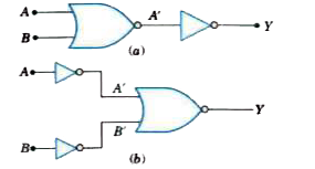
View SolutionYou are given two circuits as given below show that circuit (a) acts as OR gate while the circuit (b) acts as AND gate
View SolutionWrite the truth table for a NAND gae connected as given in the following

View SolutionWhy are elemental dopants for Silicon or Germanium usually chosen from group XIII or group XV?
View SolutionSn, C, Si and Ge are all group XIV elements . Yet , Sn is a conductor , C is an insulator while Si and Ge are semiconductors . Why?
View SolutionCan the potential barrier across a p-n junction be measured by simply connecting a voltmeter across the junction ?
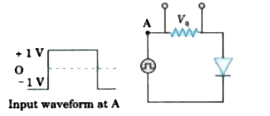
View SolutionDraw the output wave form across the resistor
View SolutionThe amplifiers `X, Y` and `Z` are connected in series. If the voltage gains of `X, Y` and `Z` are `10, 20` and `30`, respectively and the input signal is `1mV` peak value, then what is the output signal voltage (peak value)
(i) if dc supply voltage is 10V ?
(ii) if dc supply voltage is 5V?
View SolutionIn a CE transistor amplifier, there is a current and voltage gain associated with the circuit. In other words there is a power gain. Considering power a measure of energy, does the circuit violate conservation of energy ?
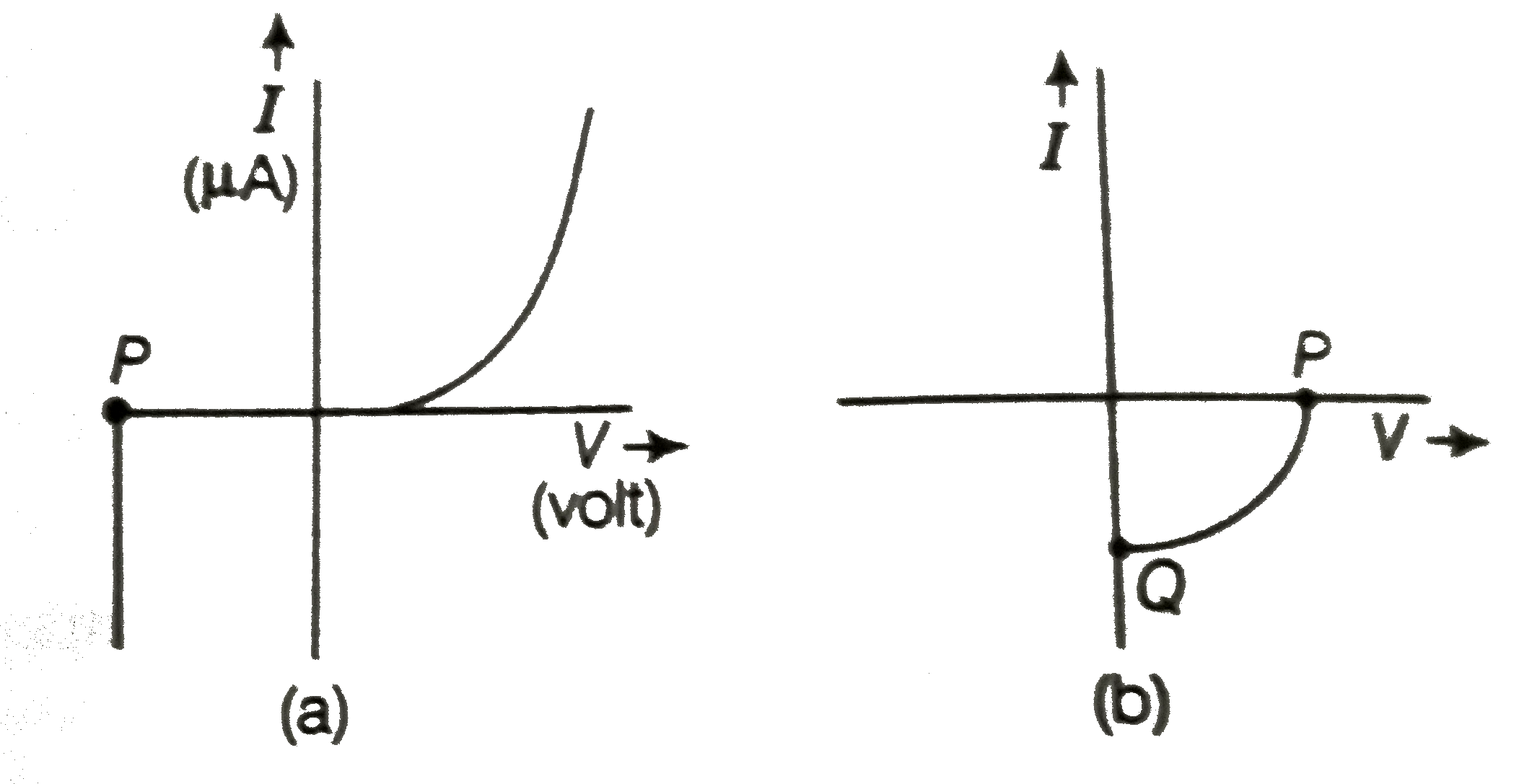
View Solution(i) Name the type of a diode whose characteristics are shown in figure (a) and (b)
(ii) What does the point P in fig. (a) represent ?
(iii) What does the point P and Q in fig. (b) represent ?
View SolutionThree photodiodes `D_1 , D_2 ` and `D_3` are made of semiconductors having
band gaps of ` 2.5 eV , 2 eV` and 3 eV , respectively . Which one will be able to detect light of wavelength ` 6000 Å ` ?
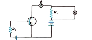
View SolutionIf the resistance `R_(1)` is increased how will the reading of the ammeter and voltmeter change
View SolutionTwo car garages have a common gate which needs to open automatically when a car enters either of the garages or cars enter both. Devise a circuit that resembles this situation using diodes for the situation .
View SolutionHow would you set up a circuit to obtain NOT gate using a transistor?
View SolutionExplain why elemental semiconductor cannot be used to make visible LEDs.
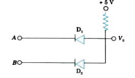
View SolutionWrite the truth table for the circuit shown in name the gate that the circuit resembles
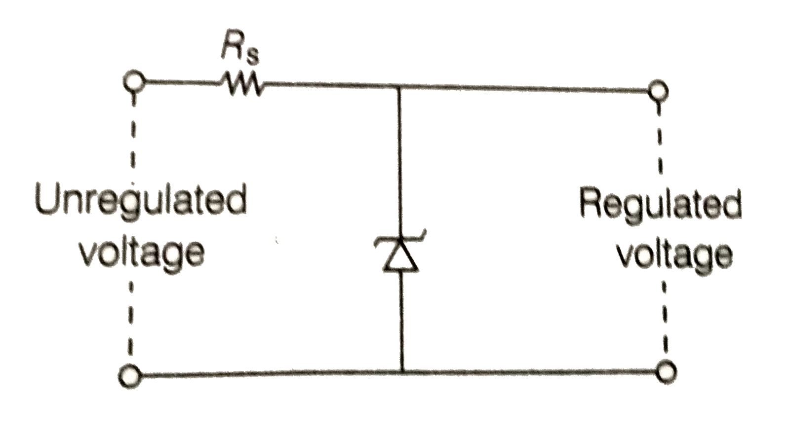
View SolutionA Zener of power rating 1 W is to be used as a voltage regulator. If Zener has a breakdown of 5V and it has to regulate voltage which fluctuated between 3 V and 7 V, what should be the value of `R_(s)` for safe operation (see figure) ?
View Solution
NCERT FILE SOLVED (TEXT BOOK EXERCISES ) questions and complete solutions for chapter SEMICONDUCTOR ELECTRONICS METERIALS DEVICES AND SIMPLE CIRCUITS of MODERN PUBLISHERS PHYSICS (HINGLISH) of Class 12
All Exercises from MODERN PUBLICATION Class 12 PHYSICS SEMICONDUCTOR ELECTRONICS METERIALS DEVICES AND SIMPLE CIRCUITS
- CHAPTER PRACTICE TEST FOR BOARD EXAMINATION
- COMPETION FILE (MULTIPLE CHOICE QUESTIONS WITH ONLY ONE CORRECT ANSWER)
- COMPETION FILE (ASSERTION REASON TYPE QUESTIONS )
- COMPETION FILE (INTEGER TYPE QUESTIONS)
- COMPETION FILE (JEE(MAIN) & OTHER STATE BOARDS FOR ENGINEERING ENTRANCE )
- COMPETION FILE (MATCHING TYPE QUESTIONS )
- COMPETION FILE (MATRIX MATCH TYPE QUESTIONS)
- COMPETION FILE (NCERT EXEMPLAR PROBLEMS :MULTIPLE CHOICE QUESTION TYPE -I)
- COMPETION FILE (NCERT EXEMPLAR PROBLEMS :MULTIPLE CHOICE QUESTION TYPE -II)
- COMPETION FILE( MULTIPLE CHOICE QUESTIONS )
- CONCEPUAL QUESTIONS
- HIGER ORDER THINKING SKILLS & ADVANCED LEVEL
- NCERT FILE SOLVED (TEXT BOOK EXERCISES )
- PRACTICE PROBLEMS
- REVISION EXERCISES (ADDITOINAL QUESTION)
- REVISION EXERCISES (NUMERICAL PROBLEMS )
- REVISION EXERCISES (SHORT ANSWER QUESTION )
- REVISION EXERCISES (VERY SHORT ANSWER QUESTION)
- REVISION EXERCISES( LONG ANSWER QUESTIONS)
- REVISION EXERCISES(FILL IN THE BLANKS )
- SOLVED EXAMPLES
- TOUGH & TRICKY PROBLEMS