Complete Solutions to SOLVED EXAMPLES of chapter SEMICONDUCTOR ELECTRONICS METERIALS DEVICES AND SIMPLE CIRCUITS of Class 12 book with complete answers and questions
| Class 12 | PHYSICS |
| Chapter | SEMICONDUCTOR ELECTRONICS METERIALS DEVICES AND SIMPLE CIRCUITS |
| MODERN PUBLICATION | SOLVED EXAMPLES |
| Number Of Questions | 40 |
| Academic Year | 2023-24 |
The number of conduction electrons in a pure semiconductor is `5xx10^(18)` per cubic metre calculte the number of holes in a sample of size `2 cm xx1 cm xx2 mm`
View SolutionEnergy of an electramagnetic radiation of wavelenght 590 nm equals the band gap of a semiconductor calculate the minimum energy required to create an electron hole pair
View SolutionA p type semiconductor has acceptor level 30 mev above the valence band what will be the maximum wavelength of light that can create a hole
View SolutionPure Si crystal at 300 k has `2.5 xx10^(28)` atoms `m^(-3)` it is doped by 1 ppm concentration of pentavalent element As calculate the new concentration of electrons and holes take `n_(i) =1.5 xx10^(16) m^(-3)`
View SolutionA semiconductor crystal has equal electron and hole concentration of `9xx10^(8) m^(-3)` it is doped by indium so that the hole concentration increases to `4.5 xx10^(12) m^(-3)` calculate the new concentration of free electrons in the doped crystal nad also mention its type
View SolutionMobilities of electrons and holes in a sample of a semiconductor is 25000 `cm^(2) V^(-1) s^(-1)` and 200 `cm^(2)` Vs respectively if the electron and hole concentration are `9 xx10^(13)` per `cm^(3)` and `4xx10^(12)` per `cm^(3)` respectively calculate the conductivity of the sample
View SolutionAn n type semiconductor of conductivity 6 `Ω^(-1) cm^(-1)` is produced when donor atoms are added to an intrinsic germanisum crystal ignoring the contributio of holes to conductivity and taking mobility of electron in n type Ge equal to 3500 `cm^(2)` /Vs determine the number density of donor atoms used for doping
View SolutionA block of intrinsic silicon at room temperature has length 0.2 m and area of cross section `4xx10^(-4) m^(2)` a battery of 3 V is connected across the block find the
(i) electron and hole currents
(ii) magnitude of total current
View SolutionThe V-I characteristic of a silicon diode is as show in the following calulate the resistance of the diode at (i) `I_(D)=15` mA and (ii) `V_(D)=10` V
View SolutionThe following table provides the set of values of V and I abtained for a given diode

Assuming the characteristics to be nearly linear and calculate the forwared and reverse bias resistance of the given diode
View SolutionThe V-I characteristics of a germainium dioide is shown in the below calculate the diode resistance in forward bias at V= +1.75 V and (b) reverse at V=-1 V

View SolutionA p-n junction diode is designed to withstand current without damage up to 5 Ma across the combination. What is the maximum voltage of the battery that can forward bias the diode safely given that the diode has a constant potential drop of 0.5 V when forward biased
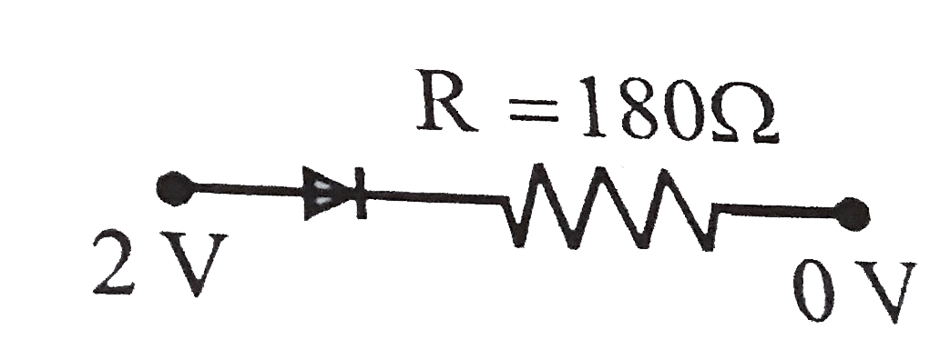
View SolutionAssuming that the silicon diode having resistance of `20 Omega`, the current through the diode is (knee voltage 0.7 V)

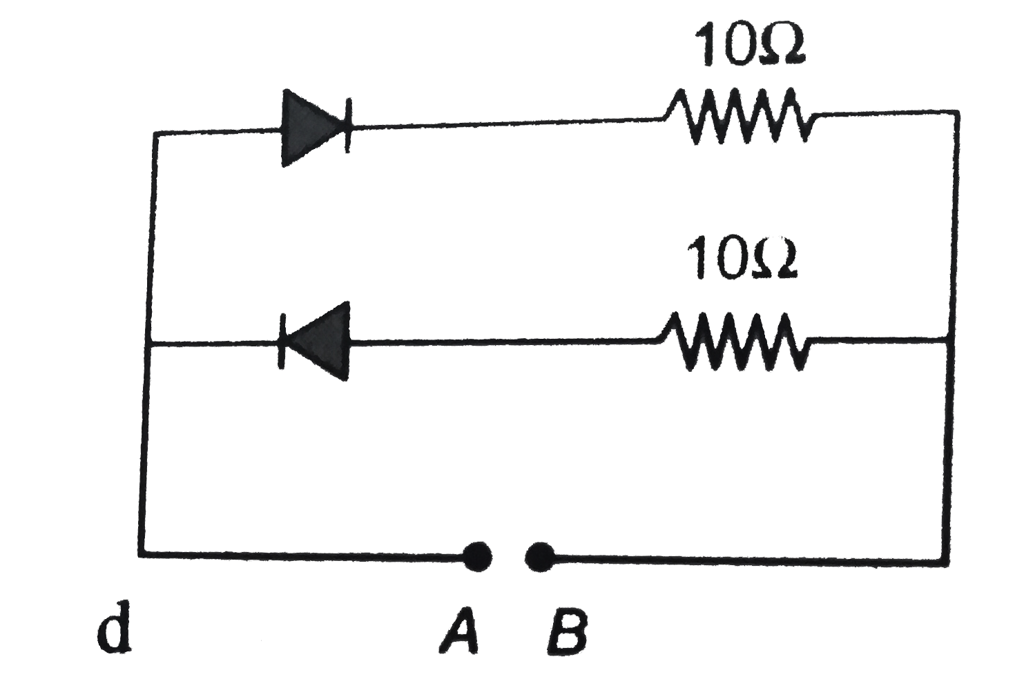
View SolutionA `2V` battery is connected across the points `A` and `B` as shown in the figure given below. Assuming that the resistance of each diode is zero in forward bias and infinity in reverse baise, the current supplied by the battery when its positive terminal is connected to `A` is

View SolutionCalculate the currents through the resistance of the circuits shown in the following figure consider the diodes to be ideal

View SolutionIn the circuite shown below calculate the curretn flowing through the cirucit and potential differnce across the diode take the drift current for the diode equal to 20 `muA`

View SolutionCompute the equivalent resistance of the circuit shown below between the points X and Y

View SolutionThe following figure shows the circuit for using zener diode of 10 V as a voltage regulator the zener diode is connected in series with a resistor r acorss a 50 V supply claculate the minimum value of r if the the maximum zener current is 25 mA

View SolutionA crystal diode of internal resistance 100 `omega` is used as a half wave rectifier as shown in the figure with AC input of V=50 sin wt and load resistance `R_(L) =1 k omega` calculate
(i) the maximum output current
(ii) DC output current (iii) DC output power

View SolutionIn a p n p transistor circuit 80% of the holes reach the collector if the collector current is 9 mA calculate the emitter and base curernts
View SolutionThe ac current gain of a transistor is 120. What is the change in the collector current in the transistor whose base current changes by `100 muA`?
View SolutionIn a common emitter transistor circuit the valtage drop across the collector is 1 V and curent gain is 70 if the collector resistor is 3 k `omega` calculate the base current
View SolutionA common emitter amplifier has a current gain of 59 if the emitter current is 5.0 mA find its base current and collector current
View SolutionCurrent gain of a transistor is 50 if the collector resistance is 5 k `omega` and input resistance is 1 k `omega` calculate the voltage gain
View SolutionIn a common emitter amplifier change in base current by 10 `muA` and collector current by `1mA` if the input resistance of the transistor is 1 `k omega` and load resistacne of `6k omega` is used in the circuit calculate
(i) the current gain
(ii) the voltage gain
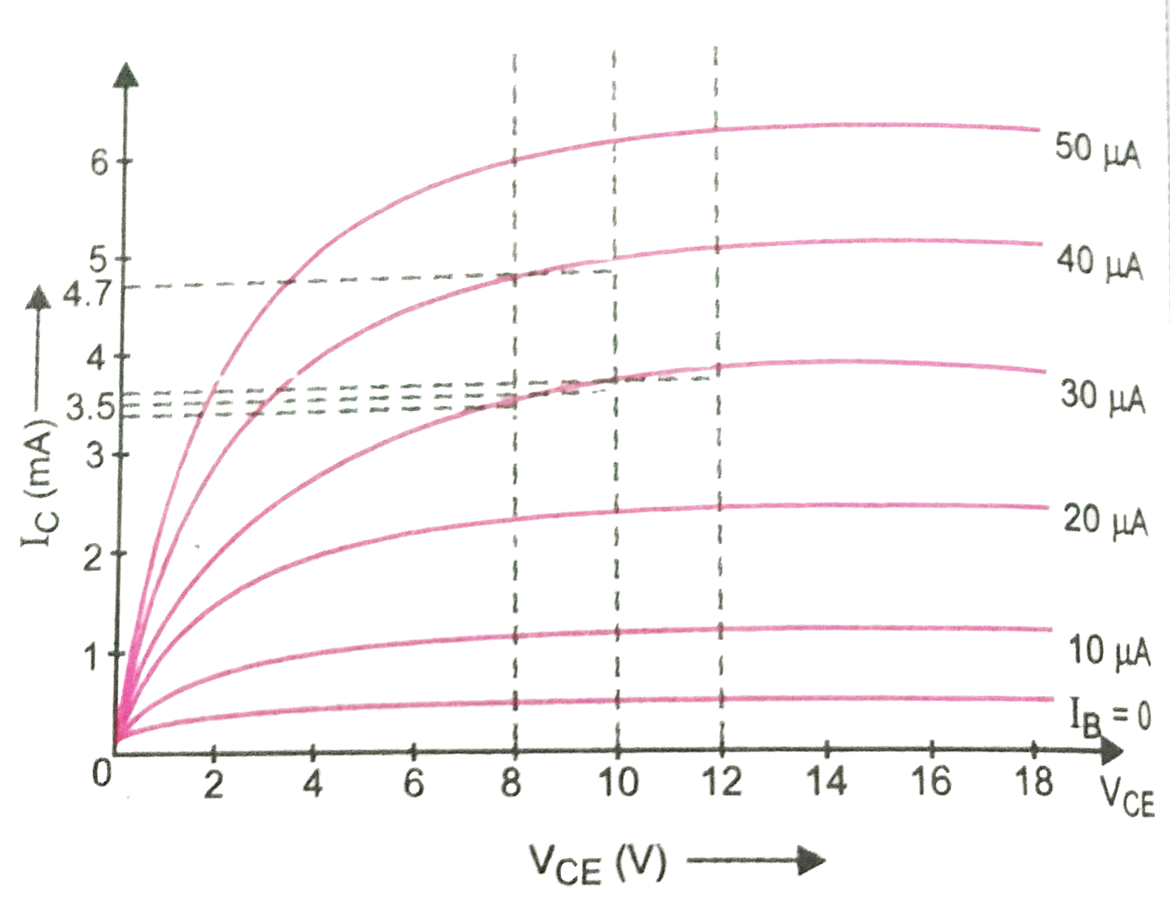
View SolutionOutput characteristics of an n-p-n transistor in CE configuration is shown in the Fig. Determine

(i) dynamic output resistance (ii) dc current gain and (iii) ac current gain at an opererating point `V_(CE)=10V`, when `I_(B)=30muA`.
View SolutionThe current gain for a common emtiter amplifier is 50 the collector resistance of the CE amplifier circuit is 2 `k omega` and input resistance is 500 `omega` if the input voltage is 0.02 V calculate the output voltage
Also calculate the power gain of the circuit
View SolutionWhen base current in a silicon transistor is changed by 12 `muA` the input resistance of the transistor is 650 `omega` when this transistor is uded as a CE amplifier with load resistance of 2 k `omega` calculate
(i) the current gain
(ii) transconductance
(iiii) voltage gain of the amplifer
View SolutionAn n p-n transistor is uded as a CE amplifier as given below if the current gain is 30 and internal resisitacne of the transistor is 100 `omega` calculate
(i) collector emitter voltage
(ii) base current
(iii) voltage gain
(iv) power gain

View SolutionIn the transistor cirucuit the base current `I_(B)=5 muA` and the collector current `I_(C )=5` mA the dc voltage of the collector circuit `V_(CC)=6V`

(i) can this circuit be used as an amplifier
(ii) If `R_(C )` is reduced to 500 `omega` can the circuit be then used as an amplifier
View SolutionAn amplifier circuit is below having an input resistance `R_(i)=25 k omega` it is connected to an external voltage vs through a eries resistance `R_(S)=50 omega` the no load voltage gain of the transistor is 150 find the apparent gain of the amplifier

View SolutionWrite the truth table for the combinatio of the gates shown name the gates used

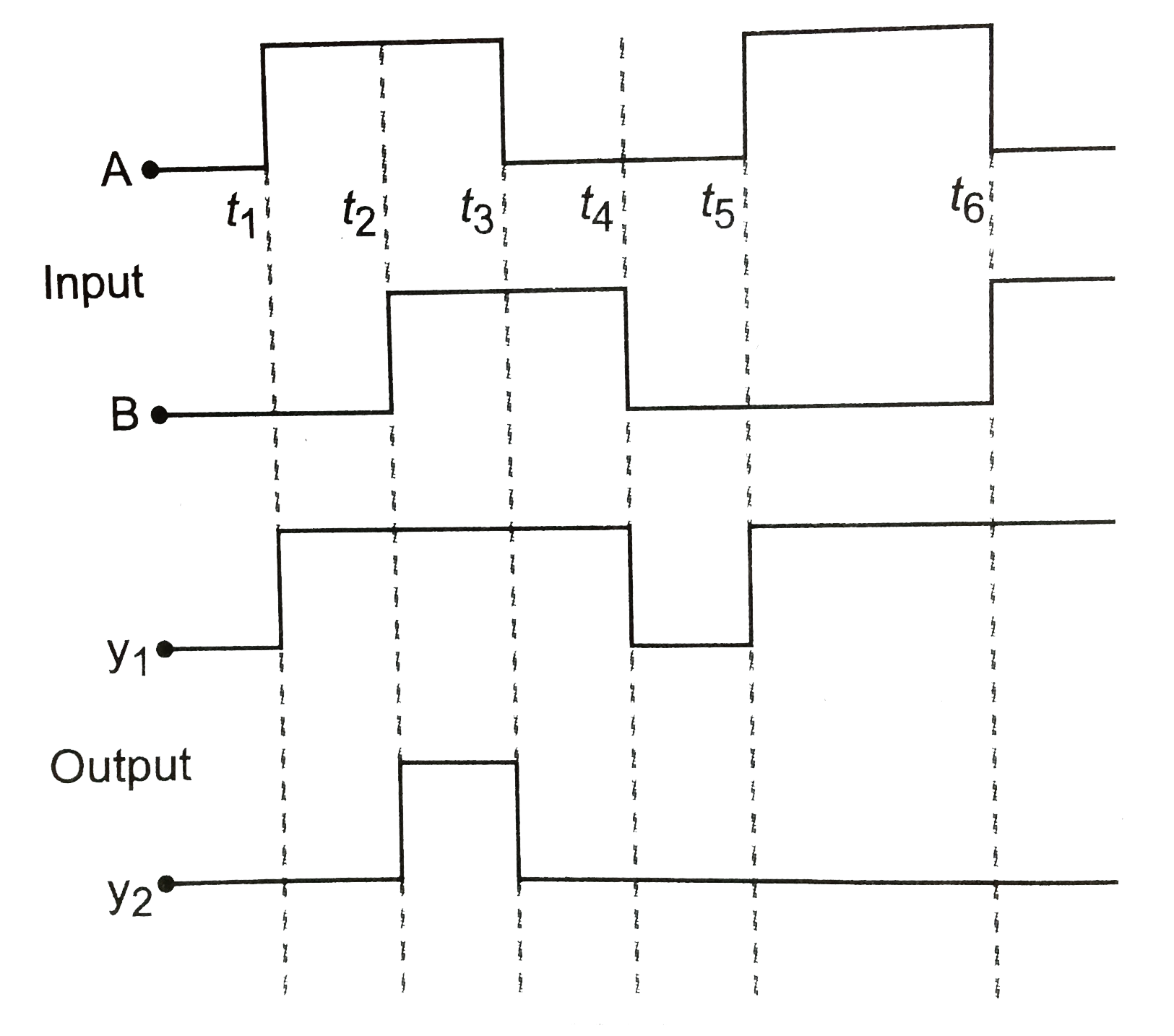
View SolutionCircuit symbol of logic gate and two input wave fronts 'A' and 'B' are in given below
(i) Name the gate used and write its truth table
(ii) Draw the output wave form

View SolutionIdentify the logic gates `G_(1)` and `G_(2)` marked in the

write down the output Y when A=1 ,B =1 and A=1 and B=0
View SolutionWrite the truth table for a NAND gate as given in Fig.9. Hence identify the exact logic operation carried out by this circuit.

View SolutionFor the given combinatin of gates find the values of ouputs `Y_(1)` and `Y_(2)` in the table given below inentify the gates `G_(1)` and `G_(2)`

View SolutionWrite the truth table for circuit given in Fig.below consisting of NOR gates and identify the logic operation (OR, AND and NOT) which this circuit is performing.

View SolutionWrite the output Y for the final circuit when
(i) A=1 and B=1
(ii) A=0 and B=0

View SolutionA student has to use an appropriate number of (i) NAND gates (only) to get the output `y_(1)` (ii) NOR gates (only) to get the output `y_(2)` from two given input A and B as shown in the Fig.

Identify the 'equivalent gate' needed in each case. Show how one can connect an appropriate number of (i) NAND (ii) NOR gates respectively in the two cases to gat the equivalent gates.
View SolutionWrite the truth table for the following circuit

View Solution
SOLVED EXAMPLES questions and complete solutions for chapter SEMICONDUCTOR ELECTRONICS METERIALS DEVICES AND SIMPLE CIRCUITS of MODERN PUBLISHERS PHYSICS (HINGLISH) of Class 12
All Exercises from MODERN PUBLICATION Class 12 PHYSICS SEMICONDUCTOR ELECTRONICS METERIALS DEVICES AND SIMPLE CIRCUITS
- CHAPTER PRACTICE TEST FOR BOARD EXAMINATION
- COMPETION FILE (MULTIPLE CHOICE QUESTIONS WITH ONLY ONE CORRECT ANSWER)
- COMPETION FILE (ASSERTION REASON TYPE QUESTIONS )
- COMPETION FILE (INTEGER TYPE QUESTIONS)
- COMPETION FILE (JEE(MAIN) & OTHER STATE BOARDS FOR ENGINEERING ENTRANCE )
- COMPETION FILE (MATCHING TYPE QUESTIONS )
- COMPETION FILE (MATRIX MATCH TYPE QUESTIONS)
- COMPETION FILE (NCERT EXEMPLAR PROBLEMS :MULTIPLE CHOICE QUESTION TYPE -I)
- COMPETION FILE (NCERT EXEMPLAR PROBLEMS :MULTIPLE CHOICE QUESTION TYPE -II)
- COMPETION FILE( MULTIPLE CHOICE QUESTIONS )
- CONCEPUAL QUESTIONS
- HIGER ORDER THINKING SKILLS & ADVANCED LEVEL
- NCERT FILE SOLVED (TEXT BOOK EXERCISES )
- PRACTICE PROBLEMS
- REVISION EXERCISES (ADDITOINAL QUESTION)
- REVISION EXERCISES (NUMERICAL PROBLEMS )
- REVISION EXERCISES (SHORT ANSWER QUESTION )
- REVISION EXERCISES (VERY SHORT ANSWER QUESTION)
- REVISION EXERCISES( LONG ANSWER QUESTIONS)
- REVISION EXERCISES(FILL IN THE BLANKS )
- SOLVED EXAMPLES
- TOUGH & TRICKY PROBLEMS