Complete Solutions to REVISION EXERCISES (SHORT ANSWER QUESTION ) of chapter SEMICONDUCTOR ELECTRONICS METERIALS DEVICES AND SIMPLE CIRCUITS of Class 12 book with complete answers and questions
| Class 12 | PHYSICS |
| Chapter | SEMICONDUCTOR ELECTRONICS METERIALS DEVICES AND SIMPLE CIRCUITS |
| MODERN PUBLICATION | REVISION EXERCISES (SHORT ANSWER QUESTION ) |
| Number Of Questions | 37 |
| Academic Year | 2023-24 |
Distinguish between intrinsic semiconductor and p-type semiconductor. Give reason, why a p-type semiconductor crystal is electrically neutral, although `n_(h)gt gtn_(e)`?
View SolutionDraw the enrgy ban diagrams of (i) n type and (ii) p type semiconductor at temperature `Tgt0K` in the case n type Si semiconductor the donor energy level is slightly below the bottom of conduction energy level is slightly above the tip of the valence band explai what role do these energy levels play in conduction and valence bands
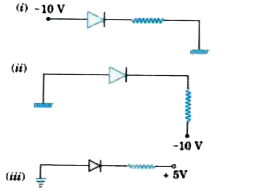
View Solutionwhich one of the two diodes is forward biased and which is reverse biased

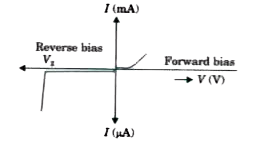
View SolutionThe figure shows the V-I characteristic of a semiconductor diode designed to operate under revese bias

(a) identify the semiconductor diode used
(b) draw the cirucuit diagram to obtain the given characteristics of this devics
(c ) briefly expain one use of this device
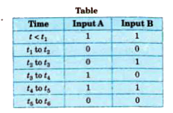
View SolutionSketch inputs A,B and output Y from a NAND gate from the table given below

View SolutionExplain with the help of a circuit diagram how the thickness of depletion layer in a p-n junction diode changes when it is forward biased
View SolutionWhat is a rectifier explain the working of P-N diode as half wave rectifier
View SolutionWhat is rectification Draw relevant circuit diagram and waveforms explain the working of p-n jucntion diode as a full wave rectifier
View SolutionName the semiconductor device that can be used to regulate an irregulation dc power supply. With the help of I-V characteristics of this device, explain its working.
View Solution(a) Draw a neat diagram showing forward biasing of a p-n junciton
Briefly explain its working draw it s V-I charcteristics for two different intensities of illumination
View Solution(a) how is a photodiode fabricated
(b) briefly explain its working draw its V-I characteristics for two different intensities of illumination
View SolutionWhat is a photodiode why is it kept in reverse bias for operation while the current available in forward bias happens to be more
View SolutionDescribe briefly using the necessary circuit diagram the three process which take place to generate the emf in a solar cell when lights falls on ti write two important criteria required for the selection of a material for solar cell fabrication
View SolutionDescribe briefly lhow light emitting diode is fabricated and expalin its working write three important advantages of LED over conventional incandescent lamps
View Solutionp-type and n-type semiconductors .
View SolutionDraw the I-V characteristics of a zener diode also sketch the circuit diagram of zener diode as a voltage regulator
View SolutionDraw a diagram of an illuninated p-n junction solar cell
View Solution(a). Explains briefly with the help of a circuit diagram how V-I characteristics of a p-n junction diode are obtainedin (i) forward bias, and (ii) reverse bias.
(b). A photo diode is fabricated from a semiconductor with a band gap of 2.8 EV. Can it detect wave length of 6000. nm? Justify.
View SolutionDraw the cirucit of full wave recitfier with capacitor filter also draw the input and output voltage of this circuit
View SolutionThe symbol of a diode is show in the figure

(a) the diode is a _________rectifier diode / photo diode / zener diode
(b) draw the VI characteristics of above diode
(c ) a zener diode with `V_(z)=6.0 V` is sued for voltage regulation if the unregulated input is 10.0 V what is the value of series resistor R
(d) what is the fundamental frequency of the ripple in a full wave rectifier cirucit operating from 50 Hz mains
View SolutionDraw the graph showing the variation of current with voltage for a p-n junctin diode when the diode is (i) forward biased and (ii) reyerse biased
View SolutionA zener diode of rating 100 mW to be used as a voltage regulator if the zener ddiode has the breakdwon voltage of 5 V and it has to regulate should be the value of `R_(S )` for safe operation

View SolutionDraw a circuit diagram of a full-wave rectifier. Explain its working principle. Draw the input/output wave forms indicating clearly the function of the two diode used.
View Solution(i) three photodiodes `D_(1),D_(2)` and `D_(3)` are made of semiconductors ahving band gaps of 2.5 eV 2eV and 3eV respecitvely which of them will not be able to detect light of wavelenghth 600nm
(ii) why phtoodiodes are required to operate in revese bias explain
View SolutionDIFFERENCE BETWEEN VALANCE BAND, CONDUCTION BAND AND ENERGY BAND
View SolutionWrite logic symbol boolean expression and truth table of AND andNOR gate
View SolutionWrite logic symbol boolean expression and truth table of NAND and OR gate
View SolutionWrite logic symbol boolean expression and truth table of NOT and OR gate ]
View SolutionWhat is a logic gate name the logic gate obtained from the figure and write its truth table

View SolutionWhat is the equivalent circuti of the combination given below answer with proper truth table

View SolutionGive the truth table for the following logic circuit

View SolutionWhat is solar cell why are Si and Ga as preferred materials for solar cell give its V-I characteristics ]
View Solution(a) Draw a neat diagram for a full wave rectifier circuit
(b) Draw the logic gate symbol and the truth table for a NAND gate with tow inputs
(c ) In an n-p-n tranasistor circuit the collector current is 10 mA if 95% of the enemitter current reach the collector what is the base current
View SolutionIn the following diagram which bulb out of `B_(1)` and `B_(2)` will glow and why

View SolutionWhat is an integrated cirucit (IC) mention the most widely used technilogy in the fabricaton of IC
View Solution(a) Draw the V-I characteristic curve for forward and reverse bias of a p-n juction diode
(b) what are th majority and ninority carriers in a p type semiconductor
(c ) wirte down the symbol and truth table of OR gate
View Solution(a) A student wants to use tow p-n junction diodes to convert alternating current in to direct curent draw the labelled circuit diagram she would use and explain how it works
(b) give the truth table and circuit symbol for NAND gate
View Solution
REVISION EXERCISES (SHORT ANSWER QUESTION ) questions and complete solutions for chapter SEMICONDUCTOR ELECTRONICS METERIALS DEVICES AND SIMPLE CIRCUITS of MODERN PUBLISHERS PHYSICS (HINGLISH) of Class 12
All Exercises from MODERN PUBLICATION Class 12 PHYSICS SEMICONDUCTOR ELECTRONICS METERIALS DEVICES AND SIMPLE CIRCUITS
- CHAPTER PRACTICE TEST FOR BOARD EXAMINATION
- COMPETION FILE (MULTIPLE CHOICE QUESTIONS WITH ONLY ONE CORRECT ANSWER)
- COMPETION FILE (ASSERTION REASON TYPE QUESTIONS )
- COMPETION FILE (INTEGER TYPE QUESTIONS)
- COMPETION FILE (JEE(MAIN) & OTHER STATE BOARDS FOR ENGINEERING ENTRANCE )
- COMPETION FILE (MATCHING TYPE QUESTIONS )
- COMPETION FILE (MATRIX MATCH TYPE QUESTIONS)
- COMPETION FILE (NCERT EXEMPLAR PROBLEMS :MULTIPLE CHOICE QUESTION TYPE -I)
- COMPETION FILE (NCERT EXEMPLAR PROBLEMS :MULTIPLE CHOICE QUESTION TYPE -II)
- COMPETION FILE( MULTIPLE CHOICE QUESTIONS )
- CONCEPUAL QUESTIONS
- HIGER ORDER THINKING SKILLS & ADVANCED LEVEL
- NCERT FILE SOLVED (TEXT BOOK EXERCISES )
- PRACTICE PROBLEMS
- REVISION EXERCISES (ADDITOINAL QUESTION)
- REVISION EXERCISES (NUMERICAL PROBLEMS )
- REVISION EXERCISES (SHORT ANSWER QUESTION )
- REVISION EXERCISES (VERY SHORT ANSWER QUESTION)
- REVISION EXERCISES( LONG ANSWER QUESTIONS)
- REVISION EXERCISES(FILL IN THE BLANKS )
- SOLVED EXAMPLES
- TOUGH & TRICKY PROBLEMS