Complete Solutions to WB JEE WORKOUT (CATEGORY 1 : Single Option Correct Type) of chapter SOLID STATE ELECTRONS of Class 12 book with complete answers and questions
| Class 12 | PHYSICS |
| Chapter | SOLID STATE ELECTRONS |
| MTG-WBJEE | WB JEE WORKOUT (CATEGORY 1 : Single Option Correct Type) |
| Number Of Questions | 30 |
| Academic Year | 2023-24 |
A `Si` and a `Ge` diode has identical physical dimensions. The band gap in `Si` is larger than that in `Ge`. An indentical reverse bias is applied across the diodes.
01:39View SolutionCarbon , silicon and germanium have four valence electrons each . At room temperature which one of the following statements is most appropriate ?
02:14View SolutionFor the given circuit of p-n junction diode which is correct?
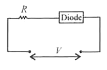 03:37View Solution
A junction diode has a resistance of 25 `Omega` when forward biased and 2500 `Omega` when reverse biased. What is the current in the diode, for the arrangement shown ?
 02:08View Solution
The peak voltage in the output of a half-wave diode rectifier fed with a sinusiodal signal without filter is `10 V`. The `dc` component of the output voltage is
01:24View SolutionA transistor is operated in common emitter configuration at constant collector voltage `V_(c)=1.5 V` such that a change in the base current from `100 muA` to `150 muA` produces a change in the collector current from `5 mA` to `10 mA`. The current gain `(beta)` is
01:56View SolutionDetermine the number density of donor atoms which have to be added to an intrinsic germanium semiconductor to produce an n-type semiconductor of conductivity `5Omega^(-1)cm^(-1)`, given that the mobility of electron in n-type germanium is `3900 cm^(2)V^(-1)s^(-1)`. Neglect the contribution of holes to conductivity.
03:21View SolutionIn a common emitter configuration, a transistor has `beta=50` and input resistance `1kOmega`. If the peak value of a.c. input is 0.01 V then the peak value of collector current is
02:08View SolutionThe following shows a logic gate circuit with two inputs A and B and the output C. The voltage waveforms of A, B and C are as shown below.
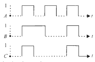
The logic circuit gate is03:54View SolutionThe current through the ideal diode as shown in the is
 01:06View Solution
The following truth table represents which type of gate?
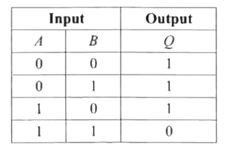 06:03View Solution
A forward biased diode is
02:20View SolutionA common emitter amplifier has a voltage gain of 50, an input impedance of `100Omega` and an output impedance of 200 `Omega`. The power gain of the amplifier is :-
01:26View SolutionIn the case of forward biasing of `PN`-junction, which one of the following figures correctly depicts the direction of flow of carriers?
02:02View SolutionThe current in the circuit will be
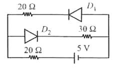 02:24View Solution
If a `p-n` junction diode, a square input signal of `10 V` is applied as shown.
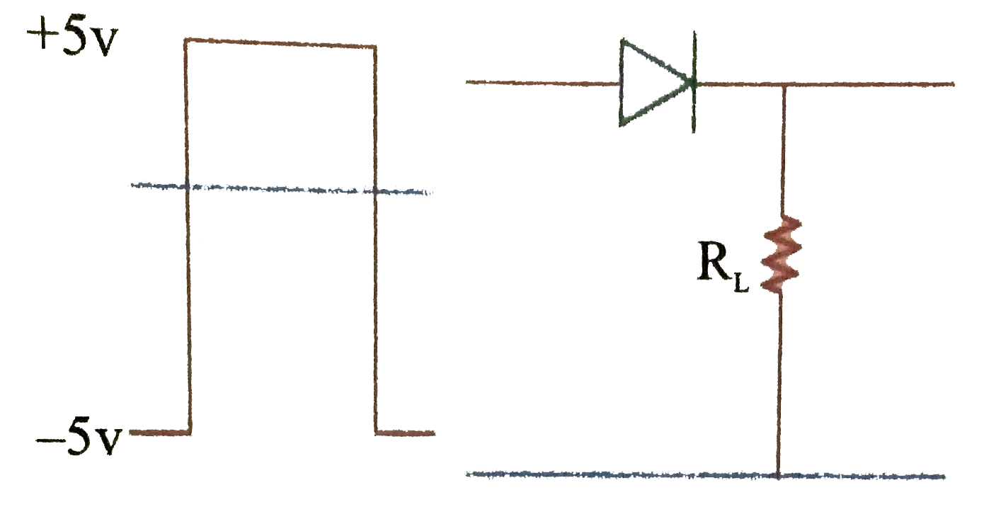
Then the out put signal across `R_(L)` will be
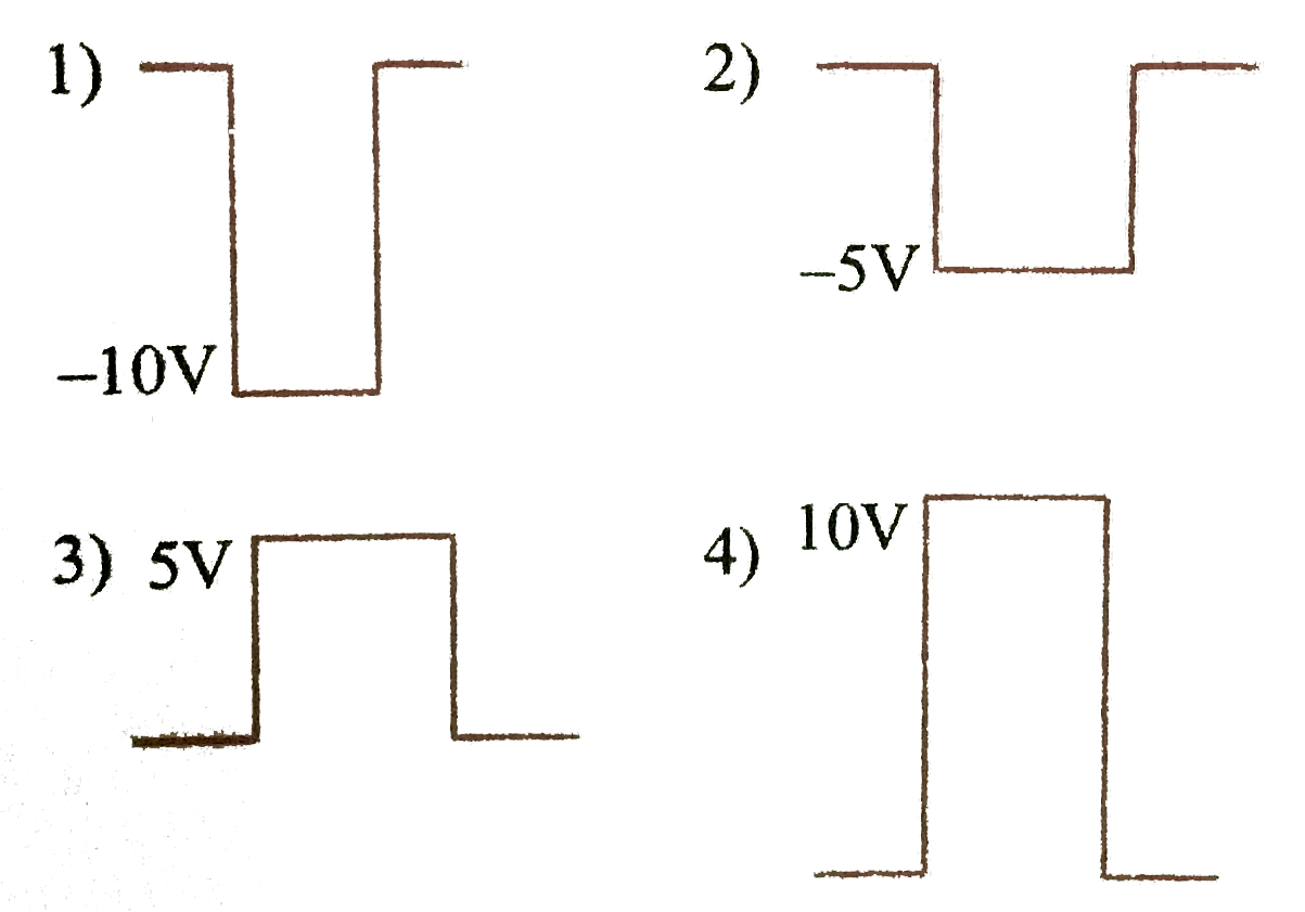 .02:56View Solution
When the forwward bias voltage of a diode is changed from `0.6` V to `0.7` V the current changes from 5 mA to 15 mA. Then its forward bias resistance is
01:43View SolutionSuppose an unregulated D.C. input voltage `V_(1)` is applied to a Zener diode having breakdown voltage `(V_(z))`. Then the breakdown condition for the diode to work as voltage regulator is
01:41View SolutionThe transfer characteristics of a base biased transistor has the operation regions, namely, cutoff, active region and saturation region. For using the transistor as an amplifier it has to operate in the
02:27View SolutionIn a transistor if collector current is 25 mA and base current is 1 mA, then current amplification factor `alpha` is
01:01View SolutionThe minimum number of NAND gates required to construct an OR gate is
03:40View SolutionIn the breakdown region, Zener diode behaves as a
01:41View SolutionDigital circuit can be made by repetitive use of
02:11View SolutionIn CE transistor amplifier if the base current is increased by `20muA,` the collector current changes from 4 mA to 5 mA. The current gain of the transistor is
03:25View SolutionAn intrinsic semiconductor has a resistivity of 0.50 `Omega` m at room temperature. Find the intrinsic carrier concentration if the mobilities of electrons and holes are `0.39 m^2 V^(-1) s^(-1)` and `0.11 m^2 V^(-1) s^(-1)` respectively
02:21View SolutionIn the following circuit Y = 1 for A and B respectively equal to
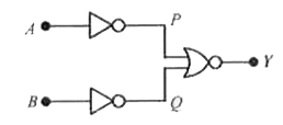 04:36View Solution
In the given circuit
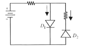 02:06View Solution
Which one of the following semiconductor diodes is reverse biased?
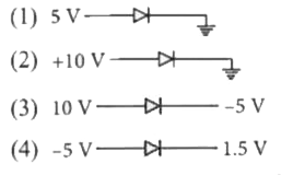 03:50View Solution
A light-emitting diode (LED) has a voltage drop of 2V across it and passes a current of `10 muA`, when it operates with a 6V battery with a limiting resistor R. what is the value of R ?
02:20View SolutionA `p-n` photodiode is made of a material with a band gap of `2.0 eV`. The minimum frequency of the radiation that can be absorbed by the material is nearly
02:47View Solution
WB JEE WORKOUT (CATEGORY 1 : Single Option Correct Type) questions and complete solutions for chapter SOLID STATE ELECTRONS of MTG-WBJEE PHYSICS (HINGLISH) of Class 12
