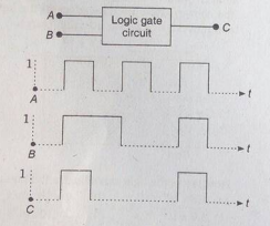
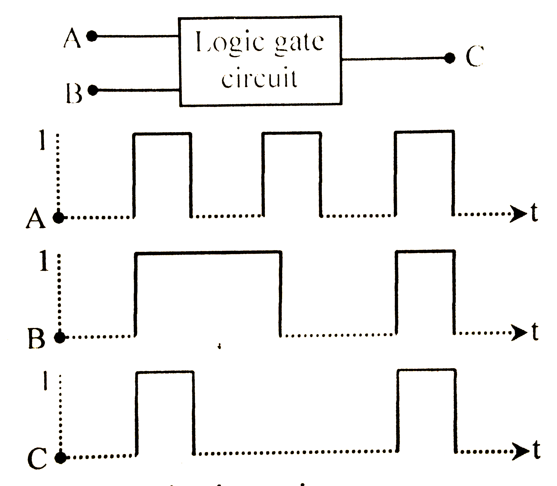
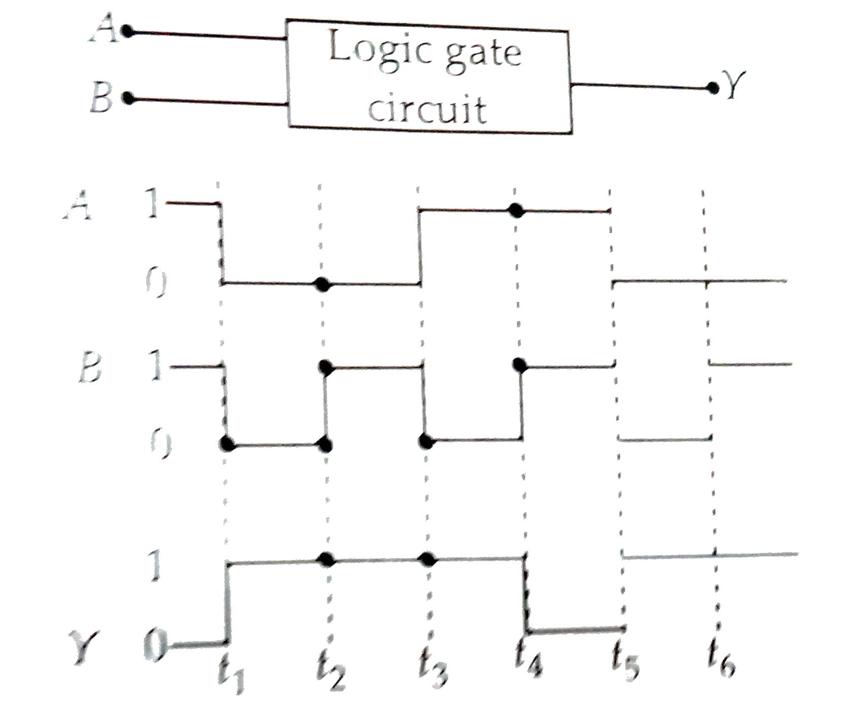
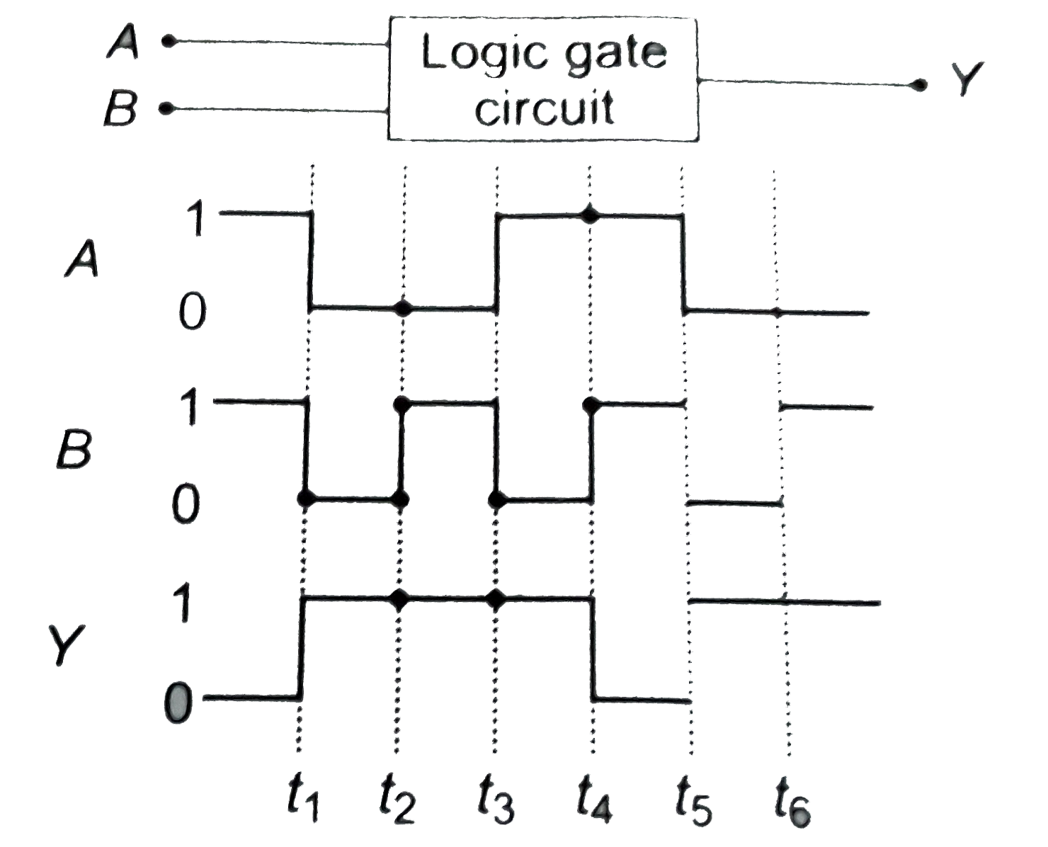
The following shows a logic gate circuit with two inputs A and B and the output C. The voltage waveforms of A, B and C are as shown below.
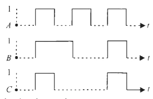
The logic circuit gate is
OR gate
AND gate
NAND gate
NOR gate
The correct Answer is:B
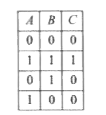
The truth table corresponding to waveform is given by
Topper's Solved these Questions
- SOLID STATE ELECTRONS BOOK - MTG-WBJEECHAPTER - SOLID STATE ELECTRONS EXERCISE - WB JEE WORKOUT (CATEGORY 3 : Single Option Correct Type)
15 Videos
- SOLID STATE ELECTRONS BOOK - MTG-WBJEECHAPTER - SOLID STATE ELECTRONS EXERCISE - WB JEE WORKOUT (CATEGORY 3 : One or More than one option Correct Type)
10 Videos
- PARTICLE NATURE OF LIGHT AND WAVE PARTICLE DUALISMBOOK - MTG-WBJEECHAPTER - PARTICLE NATURE OF LIGHT AND WAVE PARTICLE DUALISMEXERCISE - WB JEE PREVIOUS YEARS QUESTIONS
15 Videos
- THERMODYNAMICSBOOK - MTG-WBJEECHAPTER - THERMODYNAMICSEXERCISE - WB JEE Previous Years Questions
12 Videos
Similar Questions
The following figure shows a logic gate circuit with two inputs A and B and the output C. The voltage waveforms of A, B and C are as shown below.
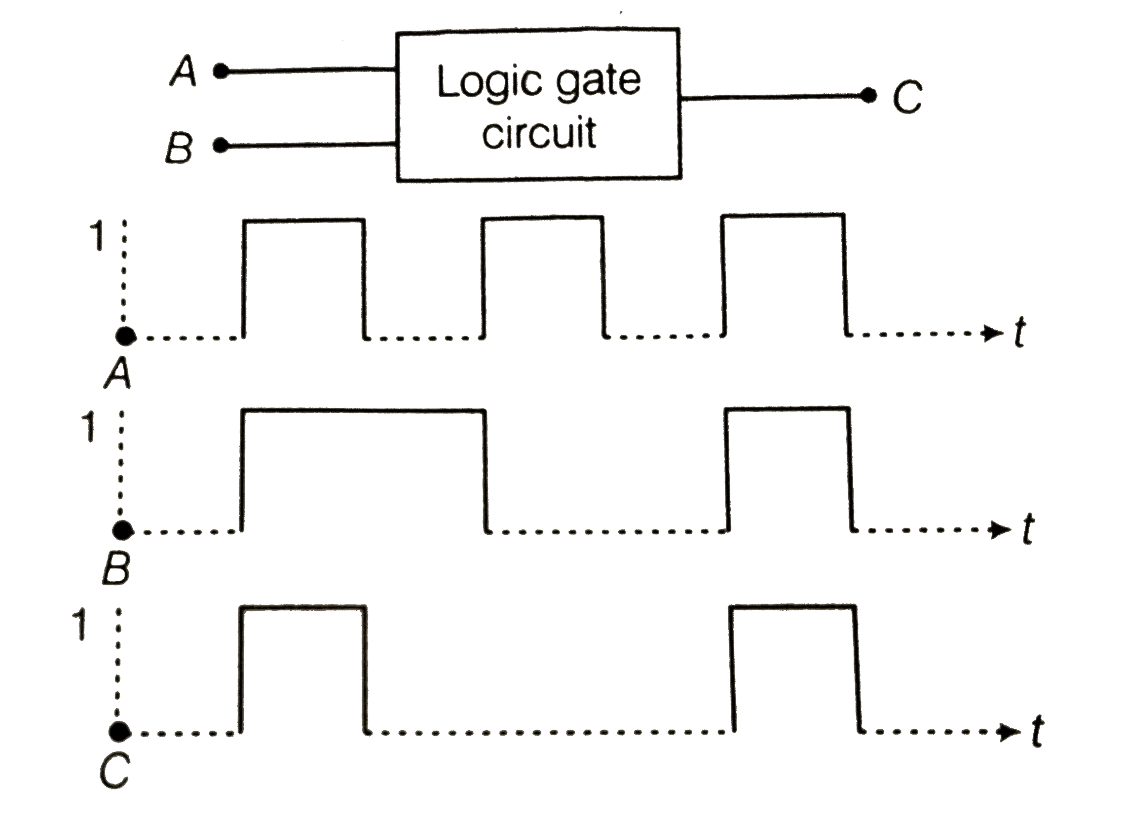
The logic circuit gate is
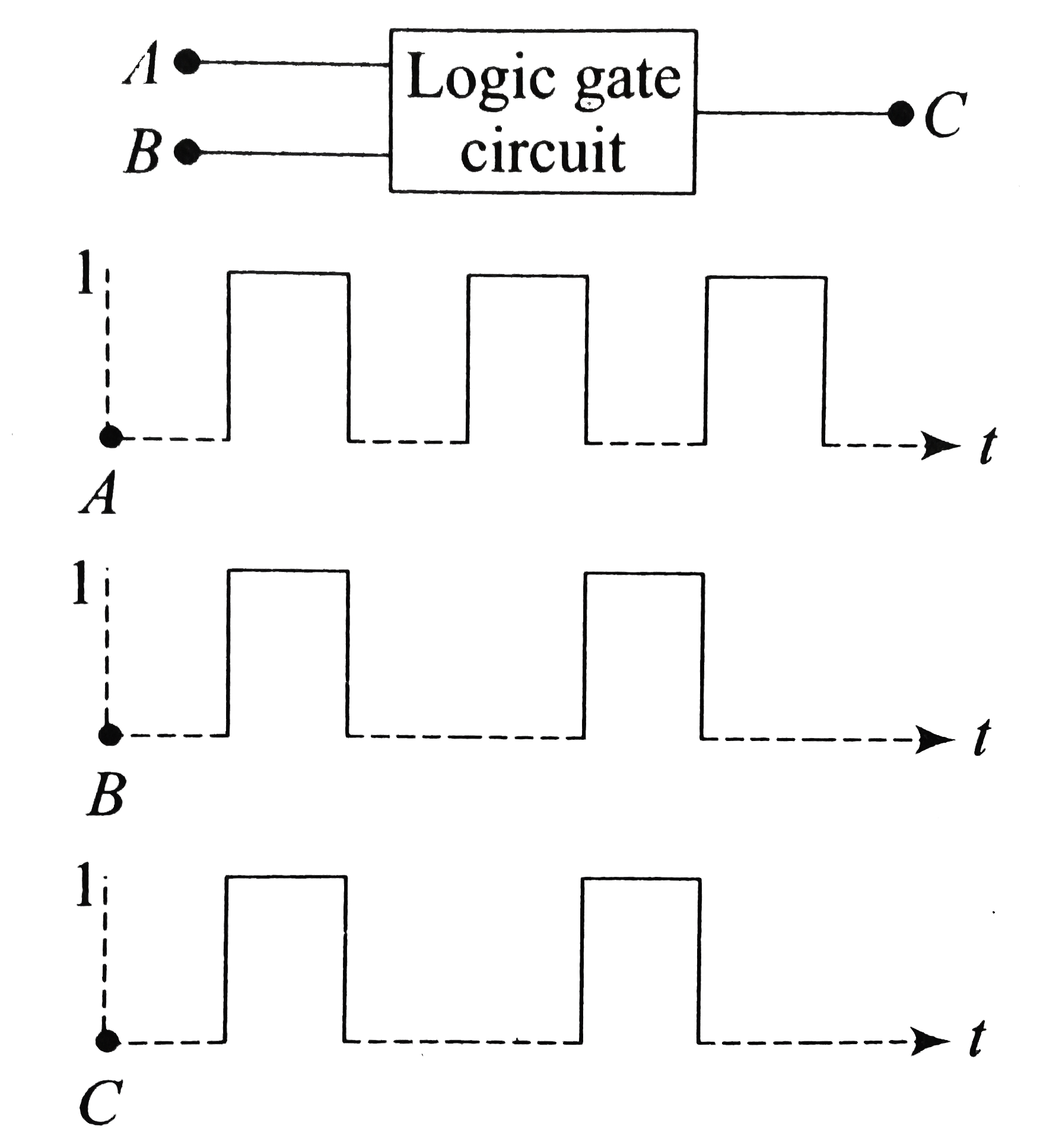
View SolutionThe following figure shows a logic gate circuit with two inputs A and B and the output C. The voltage waveforms of A,B and C are as shown below
View Solution
Knowledge Check
The following figure shows a logic gate circuit with two inputs A and B and the output C. The voltage waveforms of A, B and C are as shown below
The logic circuit gate isAAND gateBNAND gateCNOR gateDOR gateThe following figure shows a logic gate circuit with two inputs A and B and the output C. The voltage waveforms of A, B and C are as shown below

The logic circuit gate isAAND gateBNAND gateCNOR gateDOR gateThe following figure shows a logic gate circuit with two inputs A and B and the output C. The voltage waveforms of A, B and C are as shown below-
 AChange in the frequency of light into a change in electric voltageBChange in the intensity of illumination into a change in photoelectric current (CChange in the intensity of illumination into a change in the work function of the photocathodeDChange in the frequency of light into a change in the electric current
Fig, shows a logic gate circuit with two input A and B and the output C. The voltage wave form of A, B and C are as shown in Fig.The logic gate circuit is
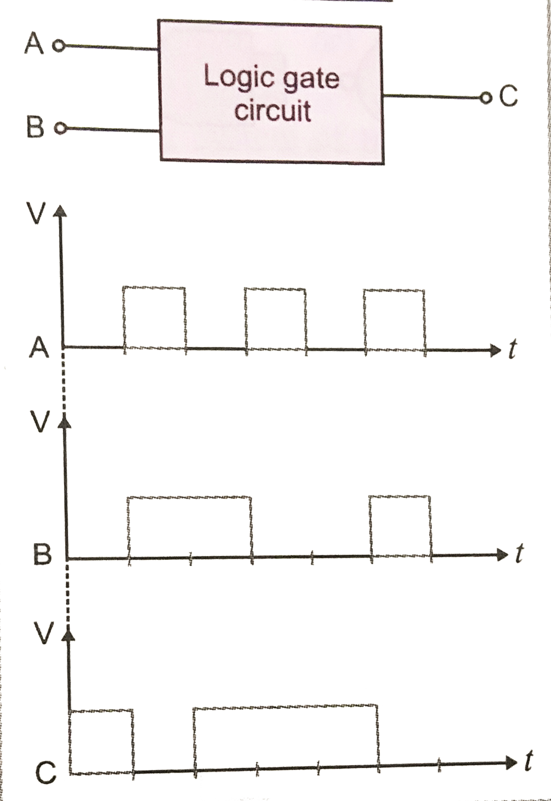
View SolutionThe figure shows a logic circuit with two inputs A and B and the output C. The voltage wave forms across A,B and C are as given. The logic circuit gate is
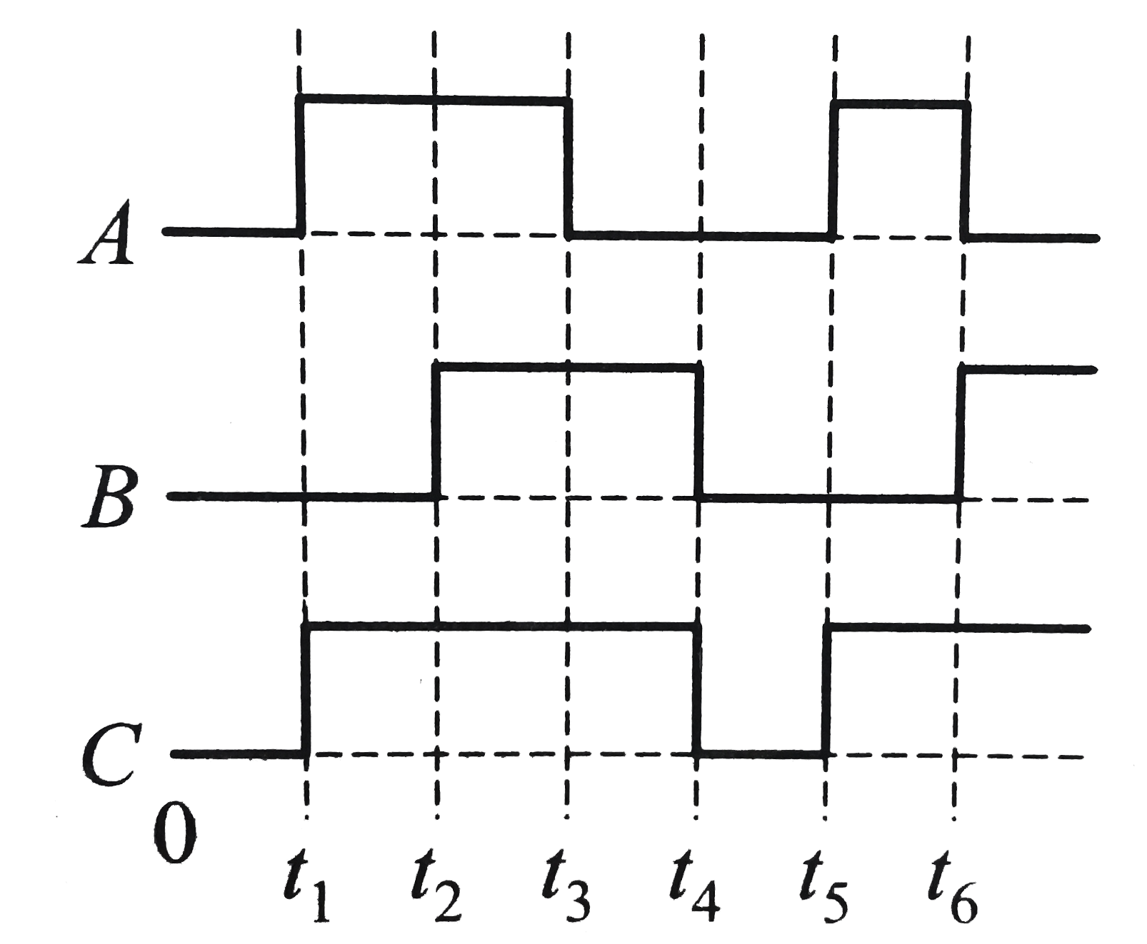
View SolutionThe following figure shows a logic gate circuit with two inputs A and B and the output Y. The voltage waveforms of A,B and Y are as given :
The logic gate is
View SolutionThe following figure shows a logic gate circuit with two inputs A and B and the output Y. The voltage waveforms of A,B and the output Y are as given
View SolutionThe figure shows a logic circuit with two inputs A and B and the output C. The voltage wave forms across A,B and C are as given. The logic circuit gate is

View Solution
