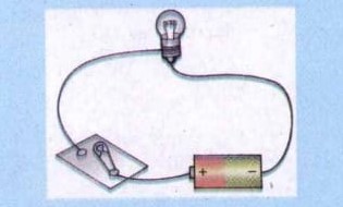

(a) Draw the circuit diagram of reversed bias p-n junction.
(b). Draw the output wavefrom across diode in given circuit.
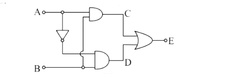
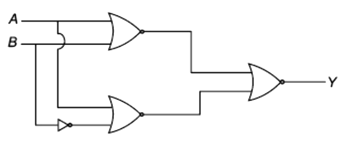
(c). Draw the truth table for the given logic gate.
Video Solution
Text Solution
(a). 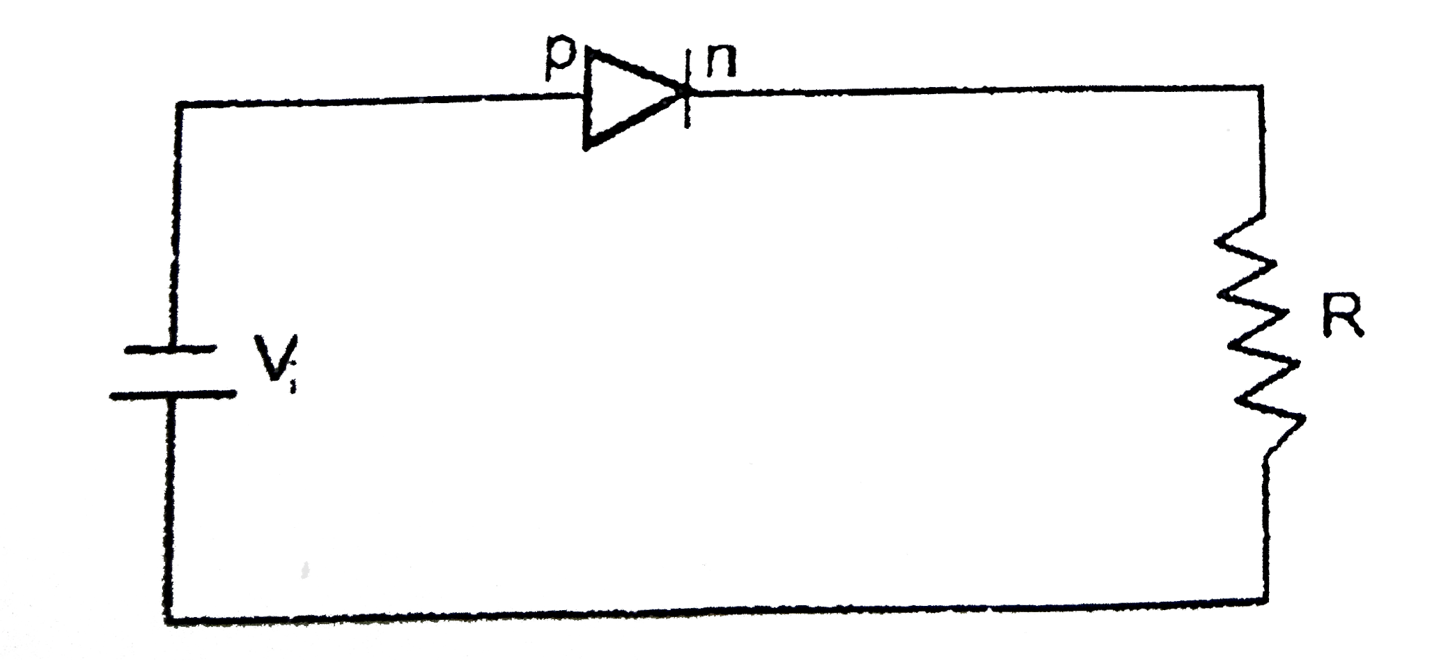
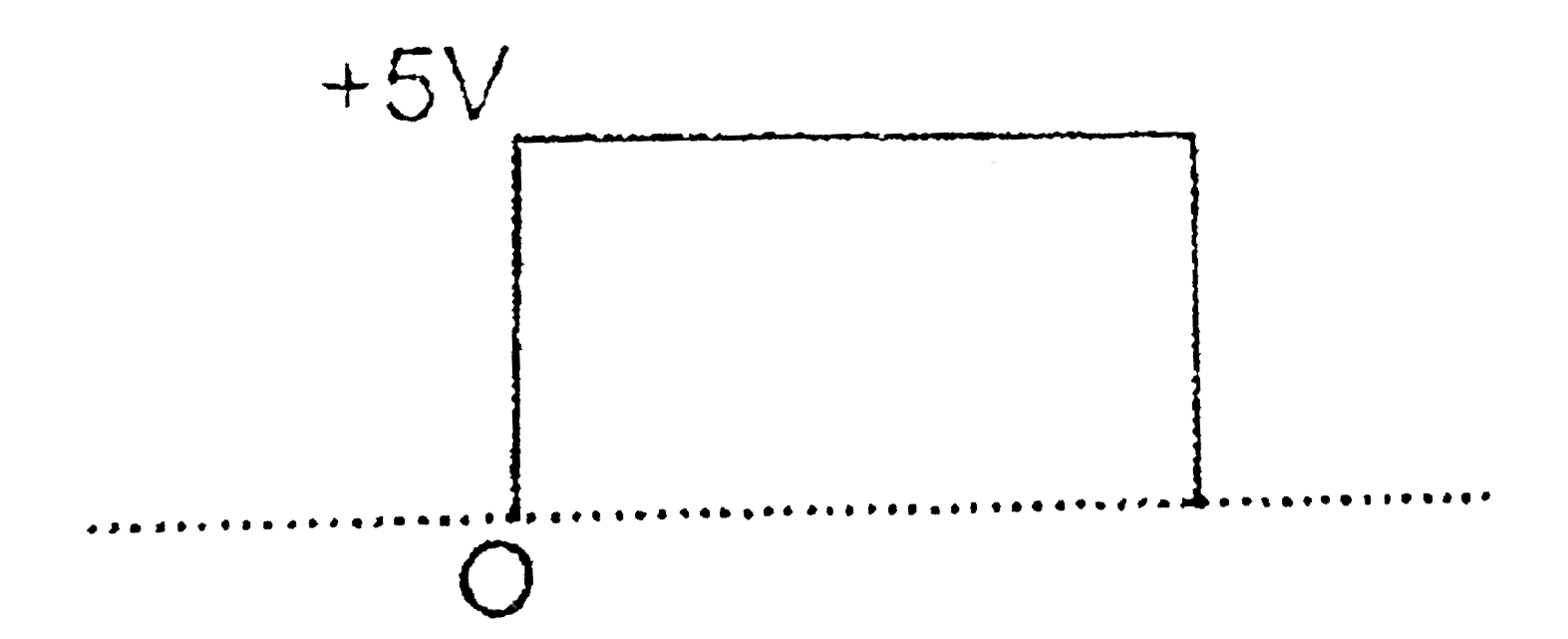
In reversed biased p-n junction positive terminal of the battery is connected to the n-side of diode and negative terminal of the battery is connected to p-side of diode.
(b). When input voltage is −5V the diode is reverse biased and no output is obtained. On the other hand when input is +5V the diode is forward biased and output is obtained which is +5V therefore,t he output wave from is shown in the figure.
(c) The given circuit is a combination of AND and NOT gate (NAND gate). The truth table will be as shown below:
ABA.BY=A.B1110010110010001
|
Updated on:21/07/2023
Topper's Solved these Questions
Similar Questions
Knowledge Check
- Question 1 - Select One
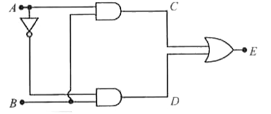
Truth table for the given circuit is
 A
A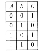 B
B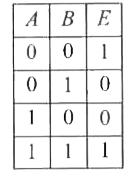 C
C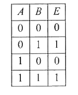 D
D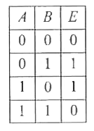
- Question 2 - Select One
Truth table for the given circuit is
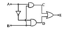 A
A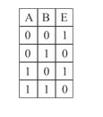 B
B C
C D
D
- Question 3 - Select One
The output of the given logic circuit is :
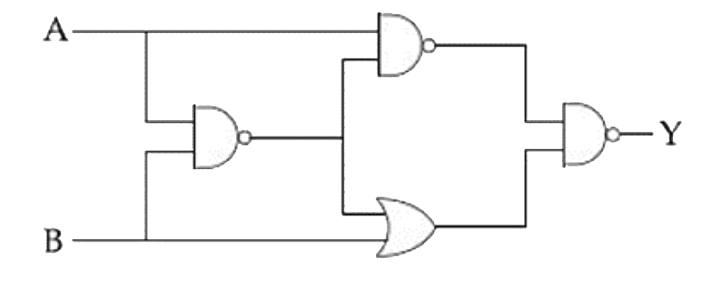 AA¯¯¯BB¯¯¯ABCAB+¯¯¯¯¯¯ABDA¯¯¯B+¯¯¯AB
The output of the given logic circuit is
 View Solution
Draw symbol and truth table for AND gate .
View SolutionDraw the circuit diagram to represent the circuit shown infigure.
 View Solution
Draw symbol and truth table for AND gate .
View SolutionDraw a diagram of an illuninated p-n junction solar cell
View Solution


