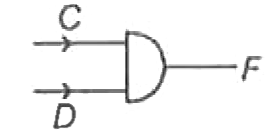
A person applies a sine wave and square wave to an AND gate as shown in the figure (i) and (ii). Assuming that both the voltages are applied in phase, the person observes the output at E and F on (i) and (ii), respectively. [Assume minimun voltage of 5 V is equivalent to logic (i)]
![A person applies a sine wave and square wave to an AND gate as shown in the figure (i) and (ii). Assuming that both the voltages are applied in phase, the person observes the output at E and F on (i) and (ii), respectively. [Assume minimun voltage of 5 V is equivalent to logic (i)]](https://d10lpgp6xz60nq.cloudfront.net/physics_images/ARH_5Y_SP_06_05_19_01_E02_038_Q01.png)
Square wave at 50 Hz and square wave at 100 Hz.
Sine wave at 50 Hz and square wave at 100 Hz
No output and sine wave at 100 Hz.
No output and pulsed wave at 100 Hz.
The correct Answer is:D
Given ,
(i) Sine weve , 50 Hz , 2 V
(##ARH_5Y_SP_06_05_19_01_E02_038_S01.png" width="80%">
(ii) sine wave , 100 Hz , 8V
In figure (i) , sine wave and square wave both have different frequency , respectively , 50 Hz and 107 Hz.
Hence , these voltages are not processed by AND gate, therefore no output is obtined from gate (i) In figure (ii), sicnce wave and square wave voltage are processed by AND gate . Since , logic gate (AND gate) gives output in two level (0 and 1) only at same frequency of input . Therefore , the output of gate (ii) will ve pulsed wave of 100 Hz.
Topper's Solved these Questions
Similar Questions
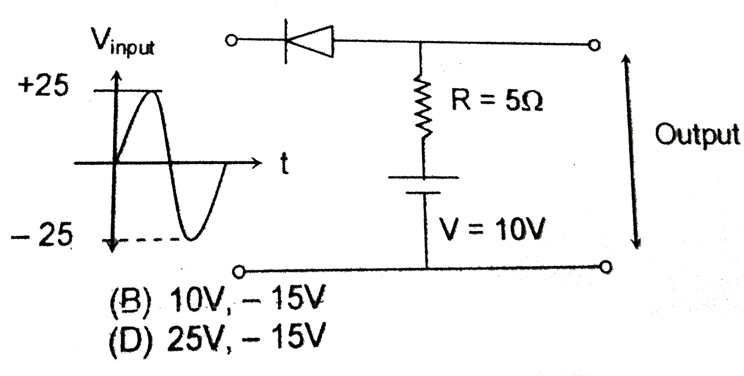
An ideal diode is connected in a circuit with resistance R=5Ω and V=10 volt as shown in figure maximum and minimum value of output voltage. When no load applied is (assume diode to be ideal)
View Solution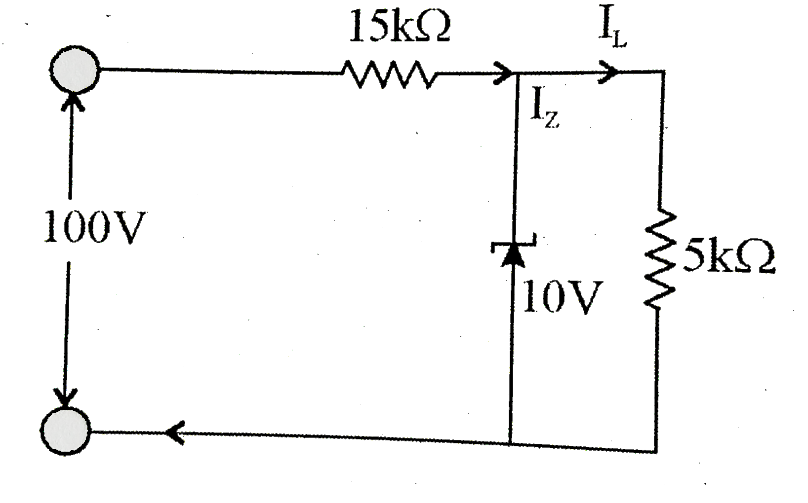
for the circuit shown in figure, find
(i). The output voltage
(ii). The votlage drop across series resistance
(iii). The current through zener diode.
View Solution
Knowledge Check

An ideal diode is connected in a circuit with resistance R=5Ω and V=10 volt as shown in figure maximum and minimum value of output voltage. When no load applied is (assume diode to be ideal)A10V, -25 VB10V, -15 VC25V,-25VD25V, -15VAn input voltage Vi of 0.20V is applied to an operational amplifier connected as shown in the diagram. What is the output voltage V0?
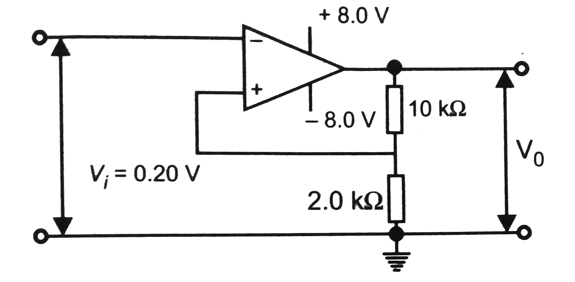 A0.20VB1.2VC0.80VD8.0V
A square wave (-1 to +1V) is applied to a P-N junction diode as shown. Draw the output wave form across the diode which is assumed to be ideal-
 A
A B
B C
C D
D
(i) Sketch the output waveform from an AND gate for the inputs A and B shown in the figure.
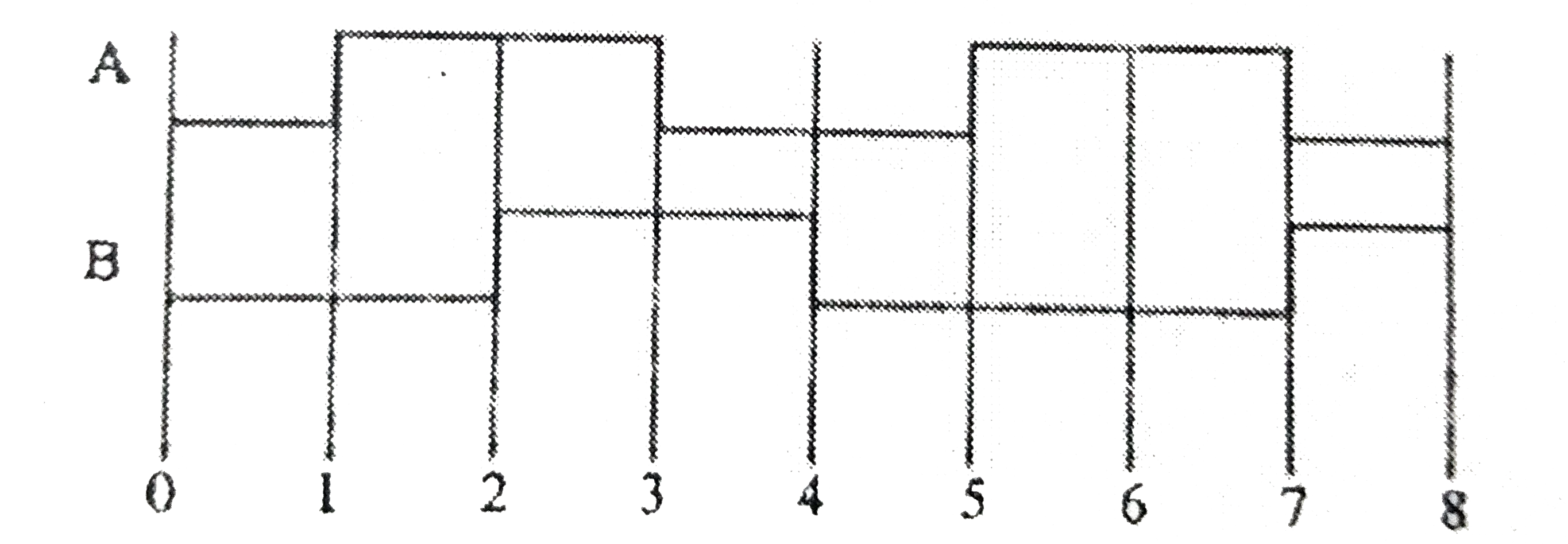
(ii) If the output of the above AND gate is fed to a NOT gate, name the gate of the combination so formed.
View SolutionFigure below shows the circuit of an electronic device :
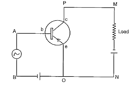
(i) Which electronic device : a rectifier, an amplifier or an oscillator does the above circuit represent?
(ii) State where the input voltage is applied and 1 where the output voltage is available.
(iii) Compare the output voltage of this circuit with its input voltage.
View SolutionA square wave (-1 to +1V) is applied to a P-N junction diode as shown. Draw the output wave form across the diode which is assumed to be ideal-

View SolutionAn amplitude modulated wave is as shown in figure. Calculate (i) the percentage modulation, (ii) peak carrier voltage and , (iii) peak value of information voltage.
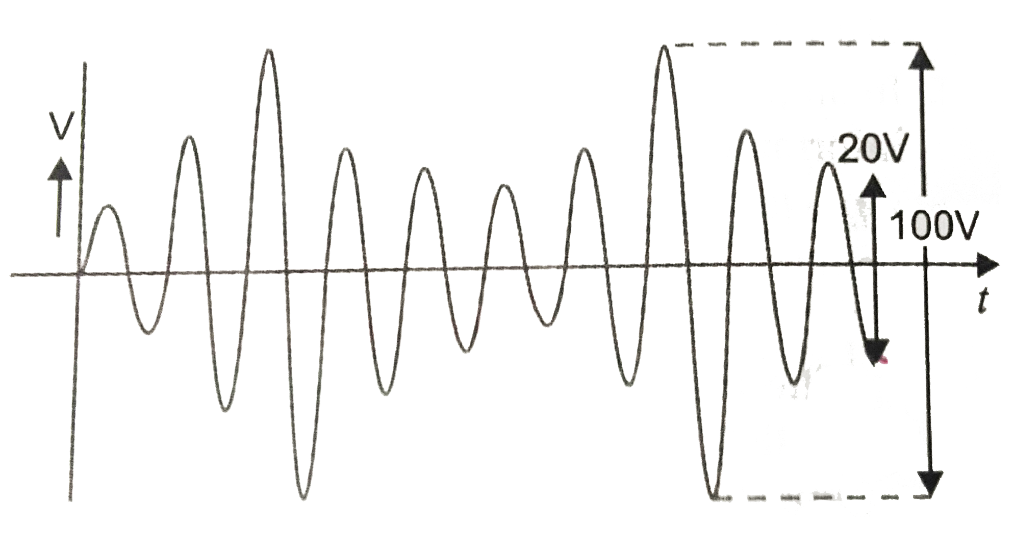
View SolutionAn amplitude modulated wave is as shown in figure. Calculate (i) the percentage modulation, (ii) peak carrier voltage and , (iii) peak value of information voltage.

View Solution
