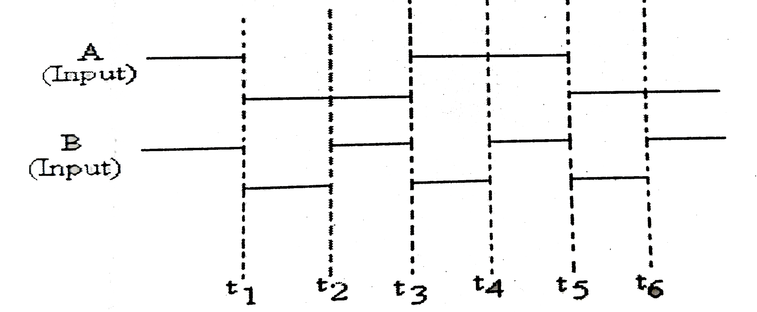
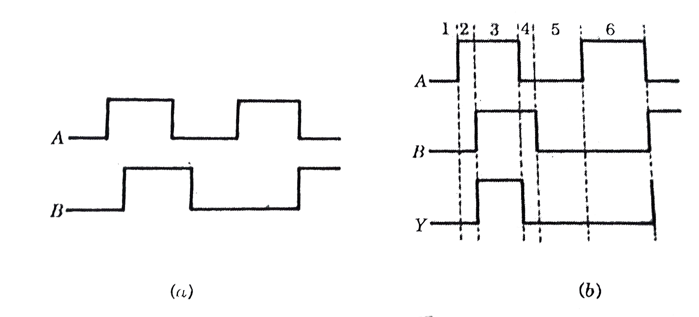
The real time variation of input signals A & B are as shown below. If the inputs are into NAND gate, then select the output signals from the following-
A
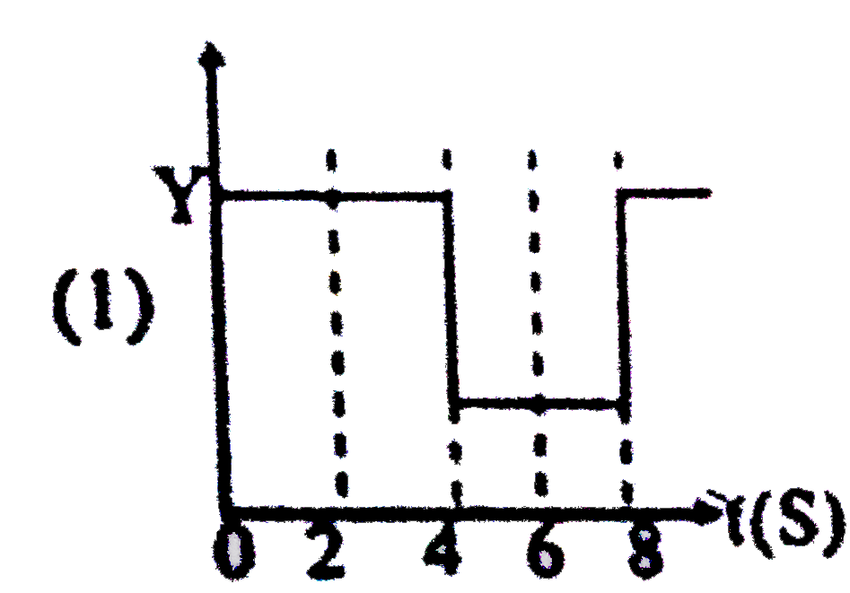
B
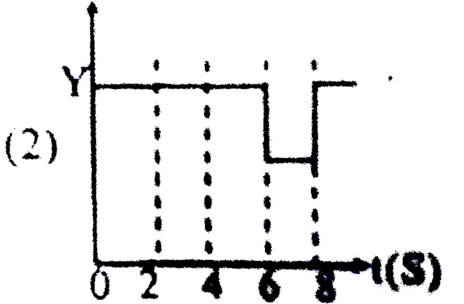
C
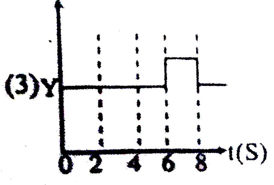
D
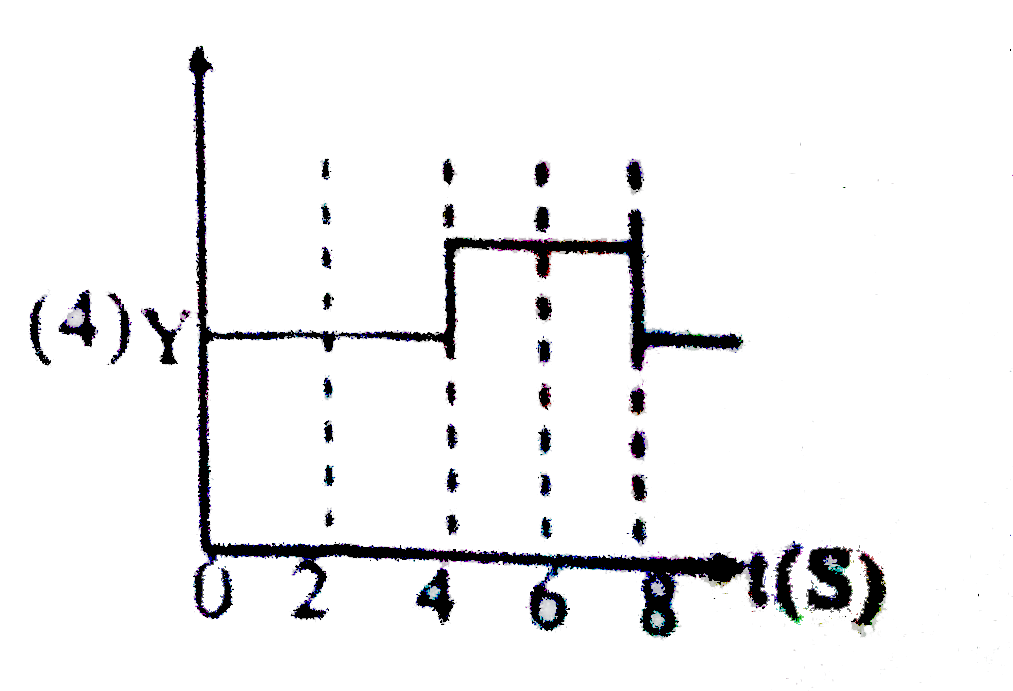
Video Solution
Text Solution
The correct Answer is:B
ABANANDB001101001110001
|
Topper's Solved these Questions
Similar Questions
Knowledge Check
The real time variation of input signals A and B are as shown below. If the inputs are fed into NAND gate, then select the output signal from the following :-
_E01_434_Q01.png) A
A_E01_434_O01.png) B
B_E01_434_O02.png) C
C_E01_434_O03.png) D
D_E01_434_O04.png)

input are given as shown
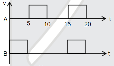
then output signal is-A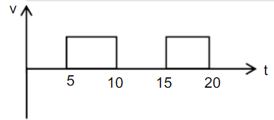 B
B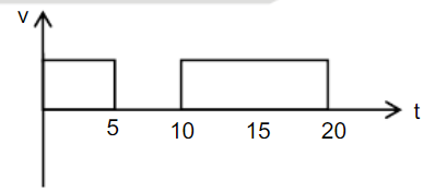 C
C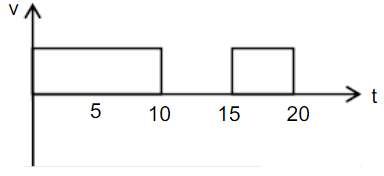 D
D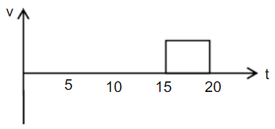
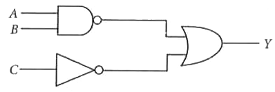
The inputs to the digital circuit are shown below. The output Y is
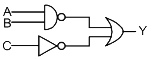 AA+B+¯¯¯CB(A+B)¯¯¯CC¯¯¯A+¯¯¯B+¯¯¯CD¯¯¯A+¯¯¯B+C
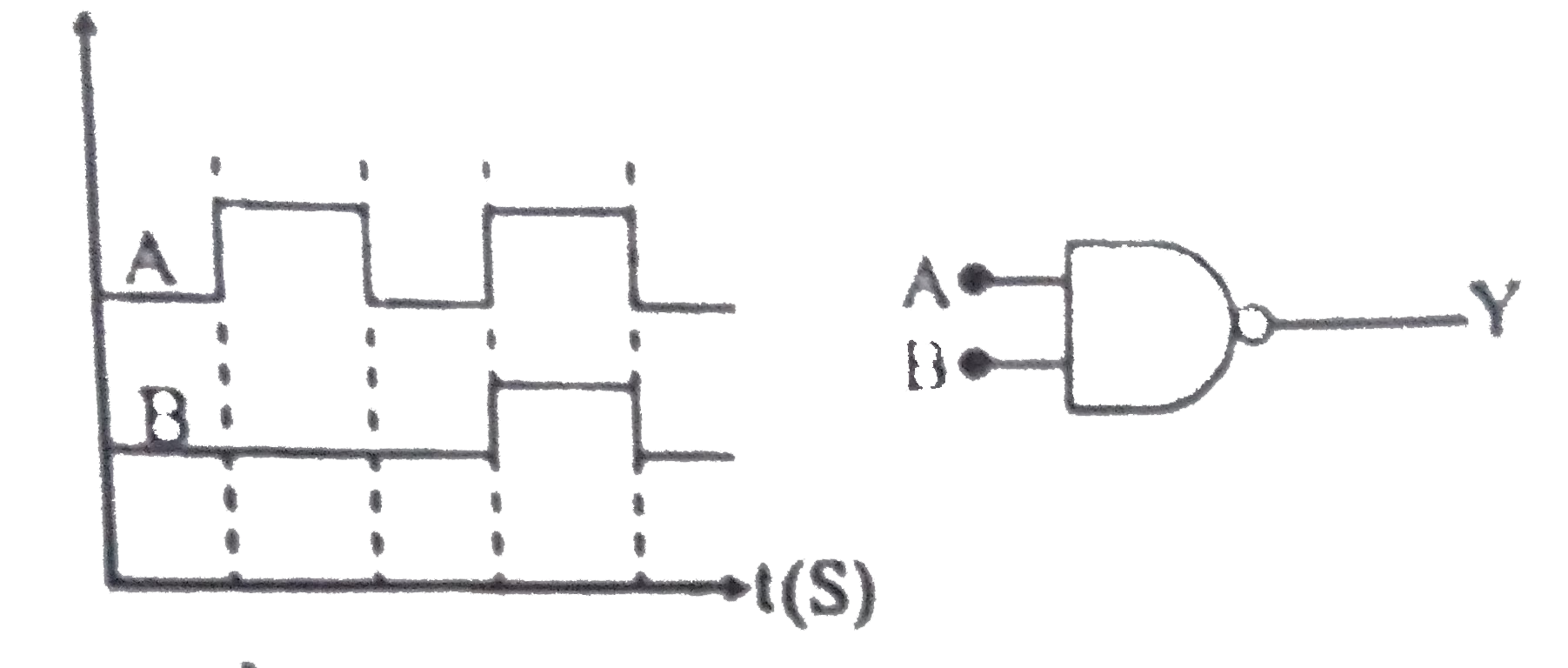
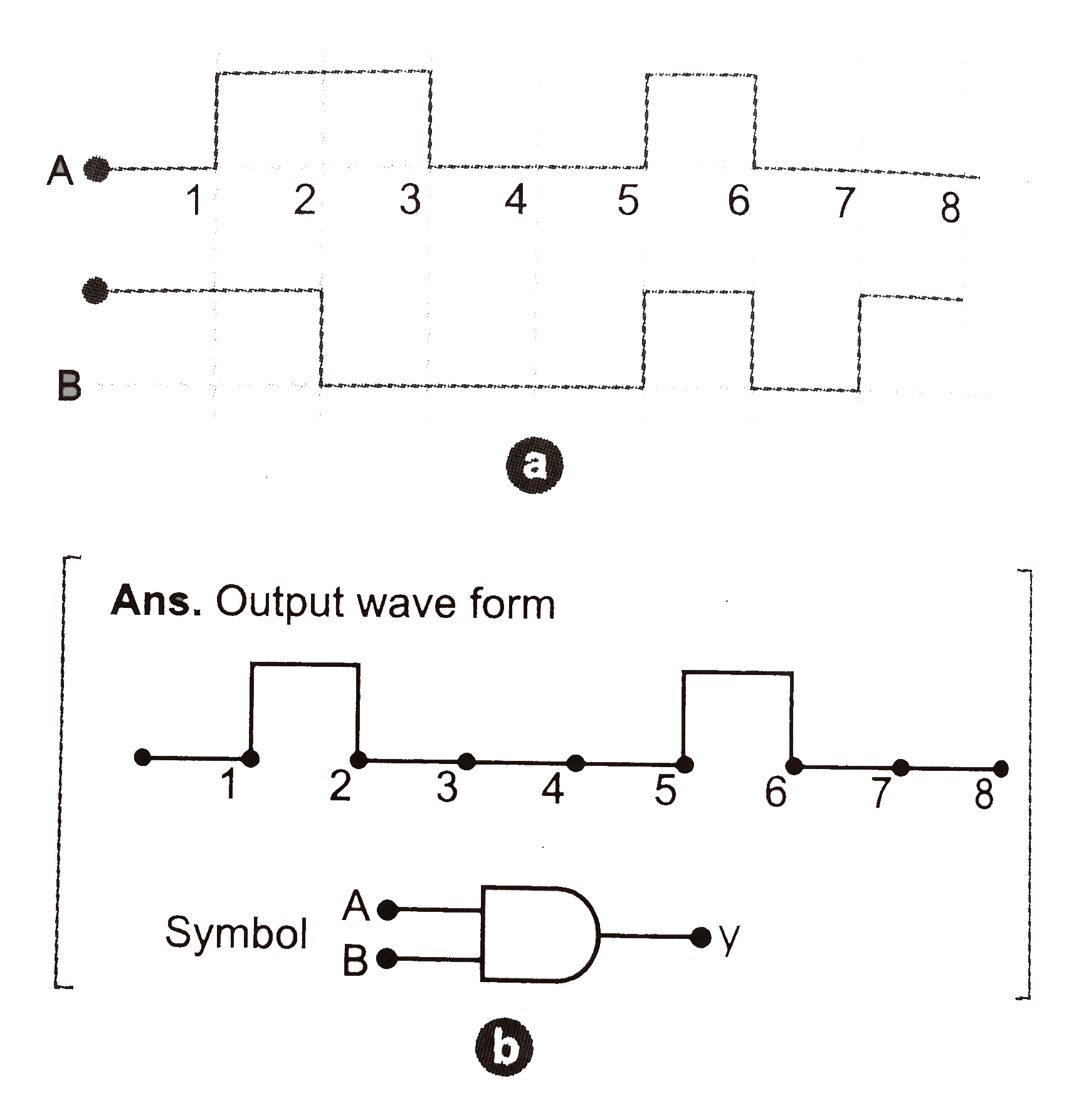
Two input waveforms A and B shown in fig (a) are applied to an AND gate.Write the output waveform.
View SolutionTwo signals A, and B shown in Fig. are used as two inputs of an AND gate obtain its output wave form. Draw the logic symblo of AND gate.
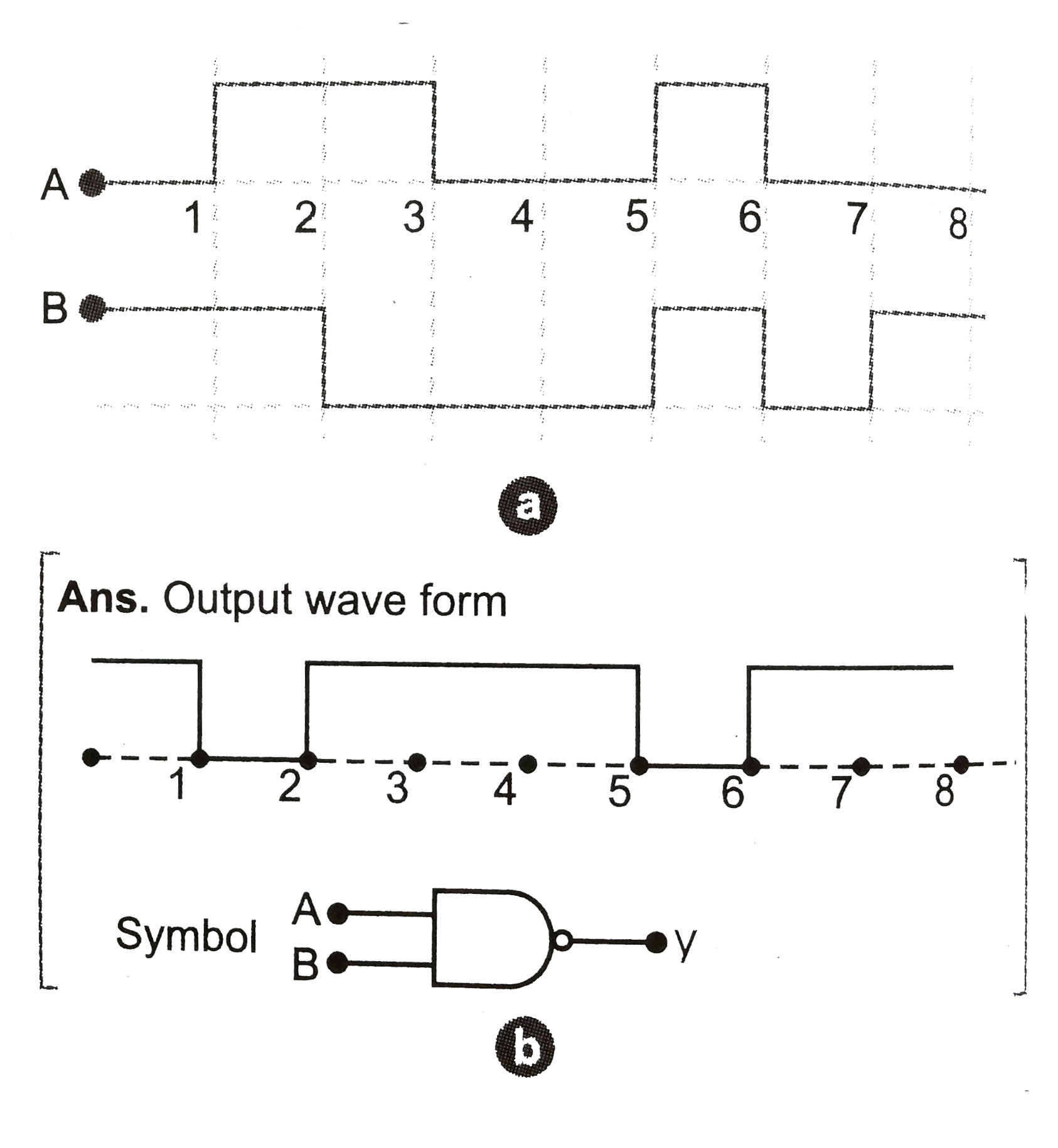
View SolutionTwo signal A and B shown in the Fig. are used as two inputs of a NAND gate. Draw its output wave form. Give the logic symbol of NAND gate.
View SolutionWhen all the inputs of a NAND gate are connected together, the resulting circuit is :-
View SolutionWhen the inputs of a two input logic gate are 0 and 0, the output is 1. When the inputs are 1 and 0, the output is zero. The type of logic gate is
View Solution

