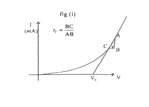
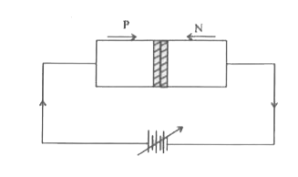
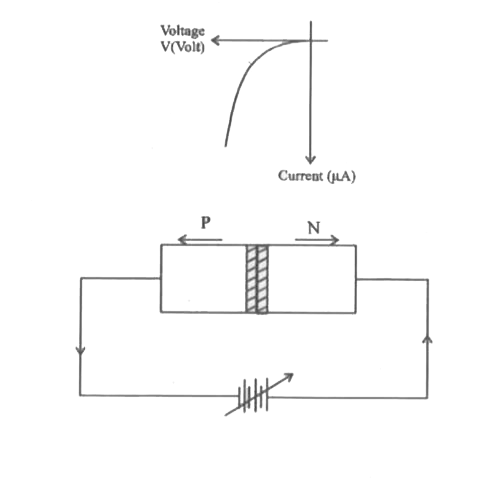
Describe with suitable block diagrams, action of pn-junction dioide under forward and reverse bias conditions . Also draw I-V characteristics .
Forward Bias : When a battery is connected across the junction such that p side is connected to the positive terminal and n side to the negative terminal of the source, the p-n junction is said to be forward biased . The applied voltage opposes the junction p.d. and for values of the applied voltage greater than the junction and constitutes a current in an external circuit. This current rises linearly with the applied voltage beyond the knee voltage . Thus a forward biased p-n junction offers a low resistance.


Reverse bias : When battery is connected across the junction such that p side is connected to the negative terminal and n side to the positive terminal , the p-n junction is said to be reverse biased In this case , the applied voltage adds to the effect of junction p.d. and hence majority carriers cannot cross the junction. The current through the circuit is practically zero. Thus , reveres bias offers a very high resistance but small current of the order of a few mA flows through the circuit due to the minority carriers in the p and n regions. As the applied voltage is gradually increased a very large current results at a particular voltage . This voltage is called the break down or cut-in voltage.

Topper's Solved these Questions
- SUPER MODEL QUESTION PAPER -5BOOK - SUBHASH PUBLICATIONCHAPTER - SUPER MODEL QUESTION PAPER -5EXERCISE - PART -D
8 Videos
- SUPPLEMENTARY EXAMINATION QUESTION PAPER (WITH ANSWER) JULY-2018BOOK - SUBHASH PUBLICATIONCHAPTER - SUPPLEMENTARY EXAMINATION QUESTION PAPER (WITH ANSWER) JULY-2018EXERCISE - PART-D
12 Videos
Similar Questions
Draw the V-I characterisitics of p-n junction diode in forward bias and in reverse bias.
View SolutionExplain briefly, with the help of circuit diagram , how V-I characteristics of a p-n junction diode are obtained in (i) forward bias, and (ii) reverse bias. Draw the shapes of the characteristic curves obtained.
Or
Explain briefly, with the help of necessary diagrams, the forward and the reverse biasing of a p-n junction diode. Also draw their characteristic curves in the two cases.
View Solution
Knowledge Check
V-I characteristics of LED is similar to forward bias characteristics of
Azener diodeBpn junction diodeCsolar cellDphoto diode
Explain briefly with the help of necessary diagram, the forward and the reverse biasing of p-n junction diode. Also draw their characteristic curves in the two cases.
View SolutionExplain briefly with the help of necessary diagram, the forward and the reverse biasing of p-n junction diode. Also draw their characteristic curves in the two cases.
View SolutionUsing the necessary circuit diagram, show how the V-I characteristics of a p-n junction are obtained in (i) forward biasing (ii) Reverse biasing. How are these characteristics made use of in rectification?
View SolutionUsing the necessary circuit diagram, show how the V-I characteristics of a p-n junction are obtained in (i) forward biasing (ii) Reverse biasing. How are these characteristics made use of in rectification?
View SolutionUsing the necessary circuit diagram, show how the V-I characteristics of a p-n junction are obtained in (i) forward biasing (ii) Reverse biasing. How are these characteristics made use of in rectification?
View Solution(a). Explains briefly with the help of a circuit diagram how V-I characteristics of a p-n junction diode are obtainedin (i) forward bias, and (ii) reverse bias.
(b). A photo diode is fabricated from a semiconductor with a band gap of 2.8 EV. Can it detect wave length of 6000. nm? Justify.
View Solution(a) Explain with the help of suitable diagram , the two processes which occur during the formations of a p -n junction diode . Hence , define the terms :
(i) depletion region and (ii) potential barrier :
(b) Draw a circuit diagram of a p - n junction diode under forward bias and explain its working .
View Solution
