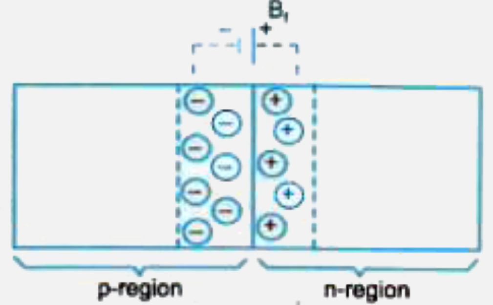
Explain with the help of a diagram the formation of depletion layer and potential barrier in a p-n junction.
Formation of depletion layer : When a p-n junction is prepared, electrons from n-region diffuse into p-region and holes diffuse from p-region to n-region. When an electron diffuses from n→ p, it leaves behind an ionised donor on n-side . This ionised donor (positive charge) is immobile as it is bonded to the surrounding atoms. Thus, due to diffhusion of electrons from n→ p, a layer of positive space charge is developed on n-side of the junction. Similarly due to diffusion of holes from p→ n a layer of negative space charge on the p-side of the junction is developed. This space charge region on either side of the junction together is known as the "depletion region" or "depletion layer".
Barrier potential: Due to diffusion of holes fromp-region to n-region and difusion of electrons in the reverse direction, part of depletion layer on n-side of junction becomes positively charged and the part of depletion layer on p-type of junction becomes negatively charged. Thus, a junction potential is developed, which opposes further diffusion of holes/electrons. Hence, this potential acts as a barrier and is known as "barrier potential" VB

Topper's Solved these Questions
- SEMICONDUCTOR ELECTRONICS : MATERIALS, DEVICES AND SIMPLE CIRCUITSBOOK - U-LIKE SERIESCHAPTER - SEMICONDUCTOR ELECTRONICS : MATERIALS, DEVICES AND SIMPLE CIRCUITSEXERCISE - LONG ANSWER QUESTIONS-I
22 Videos
- SEMICONDUCTOR ELECTRONICS : MATERIALS, DEVICES AND SIMPLE CIRCUITSBOOK - U-LIKE SERIESCHAPTER - SEMICONDUCTOR ELECTRONICS : MATERIALS, DEVICES AND SIMPLE CIRCUITSEXERCISE - SELF ASSESSMENT TEST (MULTIPE CHOICE QUESTIONS )SECTION A
3 Videos
- SEMICONDUCTOR ELECTRONICS : MATERIALS, DEVICES AND SIMPLE CIRCUITSBOOK - U-LIKE SERIESCHAPTER - SEMICONDUCTOR ELECTRONICS : MATERIALS, DEVICES AND SIMPLE CIRCUITSEXERCISE - VERY SHORT ANSWER QUESTIONS
33 Videos
- RAY OPTICS AND OPTICAL INSTRUMENTSBOOK - U-LIKE SERIESCHAPTER - RAY OPTICS AND OPTICAL INSTRUMENTSEXERCISE - SELF ASSESSMENT TEST (SECTION B)
3 Videos
- WAVE OPTICSBOOK - U-LIKE SERIESCHAPTER - WAVE OPTICSEXERCISE - SELF ASSESSMENT TEST SECTION C (VERY SHORT ANSWER QUESTIONS)
4 Videos
Similar Questions
Explain the formation of depletion layer and potential barier in a p-n junction.
View SolutionWrite the two processes that take place in the formatioin for a p-n junction. Explain with the help of a diagram, the formation of depletion region and barrier potential in a p-n junction.
View SolutionWrite the two processes that take place in the formation of a p-njunction. Explain with the help of a diagram, the formation of depletion region and barrier potential in ap-n junction.
View SolutionWrite the two processes that take place in the formation of a p-n junction. Explain with the help of a diagram, the function of depletion region and barrier potential in a p-n junction.
View SolutionExplain with the help of a diagram, how depletion region and potential barrier are formed in a junction diode.
If a small voltage is applied to a p-n junction diode how will the barrier potential be affected when it is (i) forward biased and (ii) reverse biased?
View SolutionExplain the term depletion region and potential barrier for a p-n junction.
View SolutionExplain the formation of depletion layer and potential barrier in p-n junction.
Draw the circuit diagram of a half wave rectifier and explain its working.
View SolutionExplain the formation of depletion layer and potential barrier in p-n junction.
Draw the circuit diagram of a half wave rectifier and explain its working.
View SolutionExplain with the help of a circuit diagram how the thickness of depletion layer in a p-n junction diode changes when it is forward biased
View SolutionExplain the terms 'depletion layer' and 'potential barrier' in a p-n junction diode. How are the (a) width of depletion layer, and (b) value of potential barrier affected when the p-n junction is forward biased ?
View Solution
