Draw the diagram of the circuit arangement used for studying the 'input' and the 'output' characteristics of an n-p-n transistor inits CE configuration. Briefly explain how these two types of characteristics are obtained and draw these characteristics.
(b) 'Define' the terms (i) Input resistance, (ii) Output resistance , (iii) Current amplification factor, for a given transistor.
(a) N/A
(i) The input resistance ri of the transistor in CE configuration is defined as the ratio of the small change in base -emitter voltage to the corresponding small change in the base current, when the collector-emitter voltage is kept fixed. Thus.
ri[ΔVBEΔIB]VCE=constant.
(ii) The output resistance r0 of a transistor in CE configuaration is definded as the ratio of the small change in the collector-emitter voltage to the corresponding change in the collector current when the base current is kept constant. Thus, r0[ΔVCEΔIC]IB=constant .
(ii) Current amplification factor (β) : It is defined as the ratio of the change in collector current to the small change in base current at constant collector-emitter voltage (VCE) when the transistor is in the acitve state.
βac=[ΔICΔIB]VCE=constant
Similar Questions
Knowledge Check

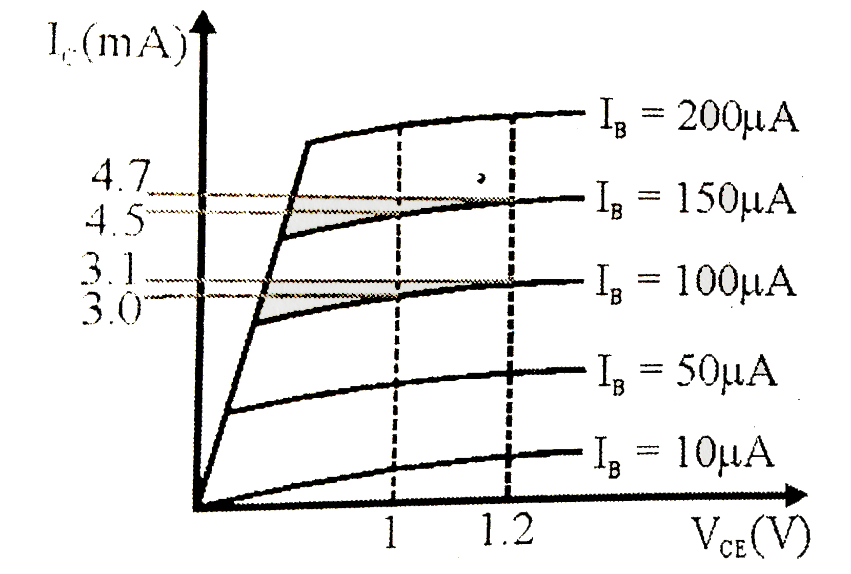
Output characteristic of n-p-n transistor in CE configuration is shown. From the characteristic curve determine the current gain at VCE=1V-A30B32C28D40
(a) Draw the circuit arrangement for studying the input and output characteristics of an n-p-n transistor in CE configuration . With the help of these characteristics define (i) input resistance , (ii) current amplification factor .
(b) Describe briefly with the help of a circuit diagram how an n-p-n transistor is used to produce self-sustained oscillations .
View Solution(i) Write the functions of three segments of a transistor.
(ii) Draw the ciruit diagram or studying the input and output characteristics of n-p-n transisfor in common emitter configuration . Using the circuit explain how input characteristics are obtained .
View SolutionDraw the typical input and output characterisitics of an n-p-n transistor in CE configurtion . Show how these characteristic can be used to determine (a) the input resistance (r1) and (b) current amplification factor (β).
View SolutionDraw a circuit diagram to obtain the characteristics of a n-p-n transistor in common base configuration . Give shape of input and output characteristic curves.
View SolutionDraw a circuit diagram to study characteristics of n-p-n transistor in CE configuration. Draw the sketch of input and output characteristics of this configuration . Define current amplification factor ?
View Solution(i) Draw a circuit diagram to study the input and output characteristics of an n-p-n transistor in its common emitter configuration. Draw the typical input and output characteristics.
(ii) Explain, with the hepl of a circuit diagram, the working of n-p-n transistor as a common emitter amplifier.
View SolutionDraw the circuit diagram for studying the characteristics of a transistor in common emitter configuration. Explain briefly and show how input and output characteristics are drawn.
View Solution
