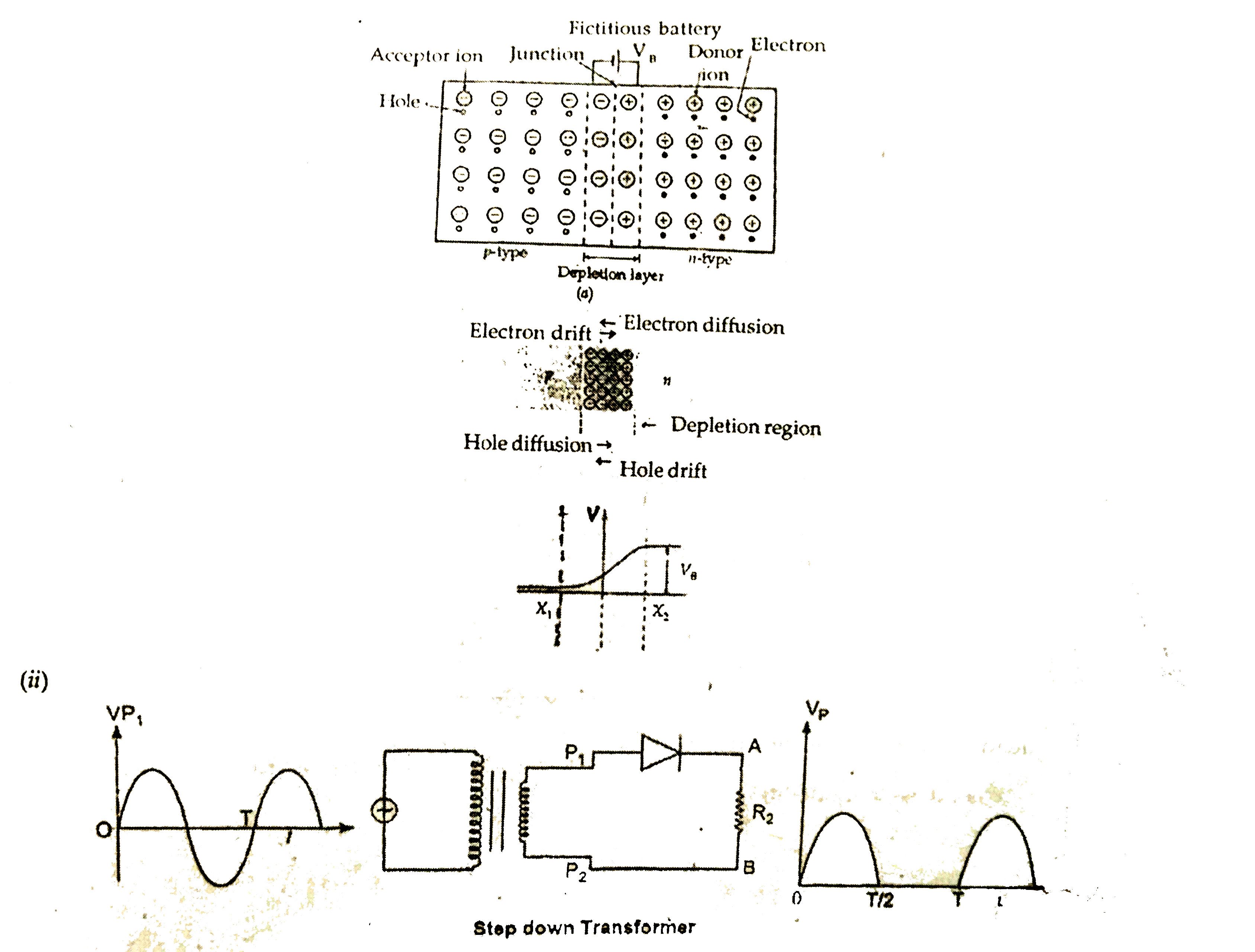
Explain the formation of depletion layer and potential barrier in p-n junction.
Draw the circuit diagram of a half wave rectifier and explain its working.
(i) The small region in the velocity of the junction which is depleted of free charge carriers and has only immobile ions is called depletion region. The accumulation of negative charges in the p-region and positive charge in the n-region sets up a potential difference across the junction. This acts as a barrier and is called barrier potential VB.

Working
(a) During positive half cycle of input alternating voltage, the diode is forward biased and a current flows through the load resistor RL and we get an ouput voltage.
(b) During other negative half cycle of the input alternating voltage, the diode is reverse biased and it does not conduct (under break down region).
Hence, AC voltage can be rectified in the pulsating and unidirectional voltage.
Similar Questions
Knowledge Check
- Question 1 - Select One
In the middle of the depletion layer of a reverse - biased p−n junction , the
Aelectron field is zeroBpotential is maximumCelectron field is maximumDpotential is zero
Explain the term depletion region and potential barrier for a p-n junction.
View SolutionDraw the circuit diagram of transistor as an oscillator and explain its working.
View SolutionDraw the circuit diagram of half wave rectifier, showing input and output voltages.
View SolutionExplain with the help of a diagram the formation of depletion layer and potential barrier in a p-n junction.
View SolutionDraw circuit diagram for a full wave rectifier and show input output voltages.
View SolutionHow is a potential barrier formed in p-n junction diode ?
View Solution(a) Define the terms depletion layer and barrier potential for a p-n junction (i) an increase in the doping concentration and (ii) biasing across the junction affect the width of the depletion layer
(b) Draw the circuit diagram of a p-n diode used a s a half wave rectifier explain its workingView Solution

