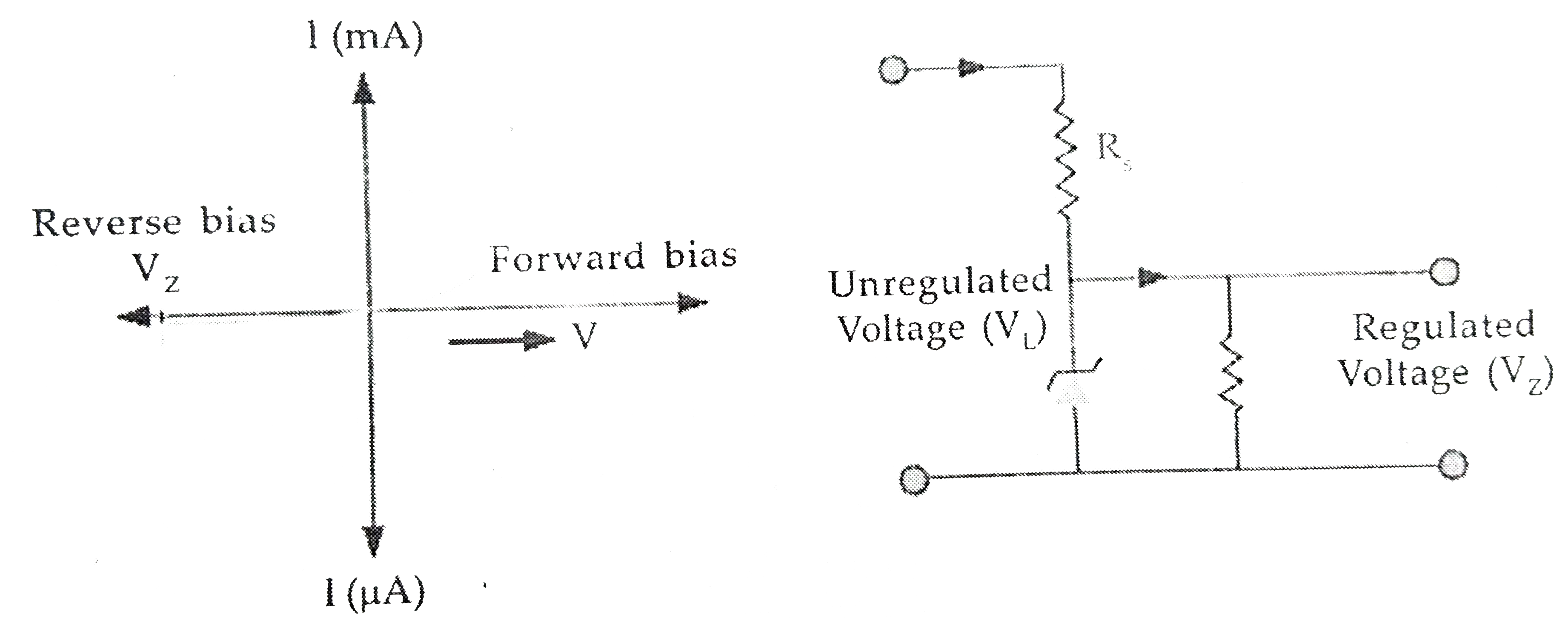
A Zener diode is fabricated by heavily doping both p- and n-sides of the junctions. Explain, why ? Briefly explain the use of zener diode as a do voltage regularor with the help of a circuit diagram.
Zener diode is fabricated by heavily doping of p−n side of junction so as to operates continuously without getting damaged in the region of reverse breakdown voltage.

Zener Diode as Voltage Regulator: Zener diode is used in regulating fluctuating voltage as shown. It is connected circuit through resistance R depending on volatage or power rating R, is connected in parallel and output is received . Om an abrupt increase of voltage across diode becomes constant, equal to breakdown voltage but current rises sharply. Hence, there is an increasein voltage drop R. As RL is in parallel so voltage across RL is same.
Topper's Solved these Questions
- XII BOARDSBOOK - XII BOARDS PREVIOUS YEARCHAPTER - XII BOARDSEXERCISE - SET-III DELHI BOARD SEC-C
5 Videos
- XII BOARDSBOOK - XII BOARDS PREVIOUS YEARCHAPTER - XII BOARDSEXERCISE - [SET -II, OUTSIDE DELHI]
9 Videos
- XII BOARDSBOOK - XII BOARDS PREVIOUS YEARCHAPTER - XII BOARDSEXERCISE - SET-II DELHI BOARD (SEC-B)
2 Videos
- SAMPLE PAPER 2019BOOK - XII BOARDS PREVIOUS YEARCHAPTER - SAMPLE PAPER 2019EXERCISE - SECTION D
6 Videos
Similar Questions
A Zener diode is fabricated by heavily doping both p- and n-sides of the junctions. Explain, why ? Briefly explain the use of zener diode as a dc voltage regulator with the help of a circuit diagram.
View SolutionA zener diode is fabricated by heavily doping both p- and -sides of the junction. Explain why ? Breifly explain the use of zener diode as a d.c. voltage regulator with the help of a circuit diagram.
View Solution
Knowledge Check
Zener diode has both p and n-ends heavily doped so that-
Ait has small thickness of depletion regionBit has large thickness of depletion region due to large recombinationCit has large reverse bias voltageDit has weak reverse current when reverse biasedZener diode is a p-n junction which has-
Ap-end heavily doped,n-end lightly dopedBn-end heavily doped, p-end lightly dopedCboth p and n-ends heavily dopedDboth p and n-ends lightly dopedWhen used in a circuit, Zener diode is always
Aforward biasedBreverse biasedCboth forward and reverse.Dconnected inseries.
ZENER DIODE AS VOLTAGE REGULATOR
View SolutionZener diode is fabricated by heavily doping both p- and n-sides of the junction so breakdown occurs at a voltage of about 5 V in reverse bias.
View SolutionWhat is Zener diode? How is it used as voltage regulator?
View SolutionDraw a lablled circuit diagram of a Zener diode as a voltage regulator.
View SolutionZener diode is a specially desined p-n junction diode, in which both p-side and n-side of p-n junction are heavily doped. The zener diode is designed especially to operate in the reverse break down voltage region continuosly without being damaged? Zener diode is used to remove the fluctuations from the given voltage and thereby provides a voltage of constant magnitude (i.e., Zener diode is used as voltage regulator).
Read the above pragraph and answer the following question:
(i) What is the most important use of Zener diode?
(ii) What are the essential conditions for proper working of Zener diode?
(iii) What do you learn from the above atudy?
View Solution
