(a) Draw the circuit diagram of a full wave rectifier using p-n junction diole. Explain its working and show the output, input waveforms.
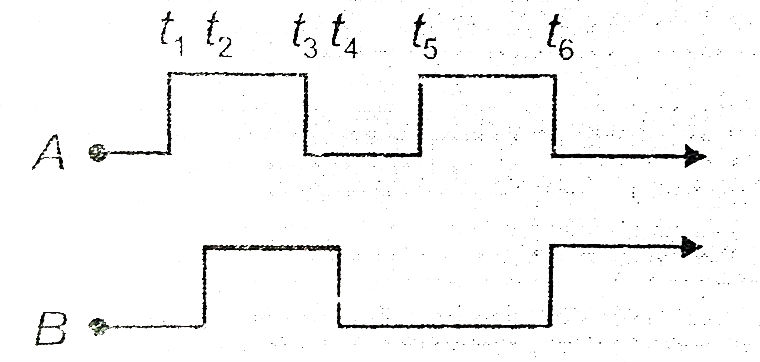
(b) Show the output waveforms (Y) for the following inputs A and B of (i) OR gate (ii) NAND gate :
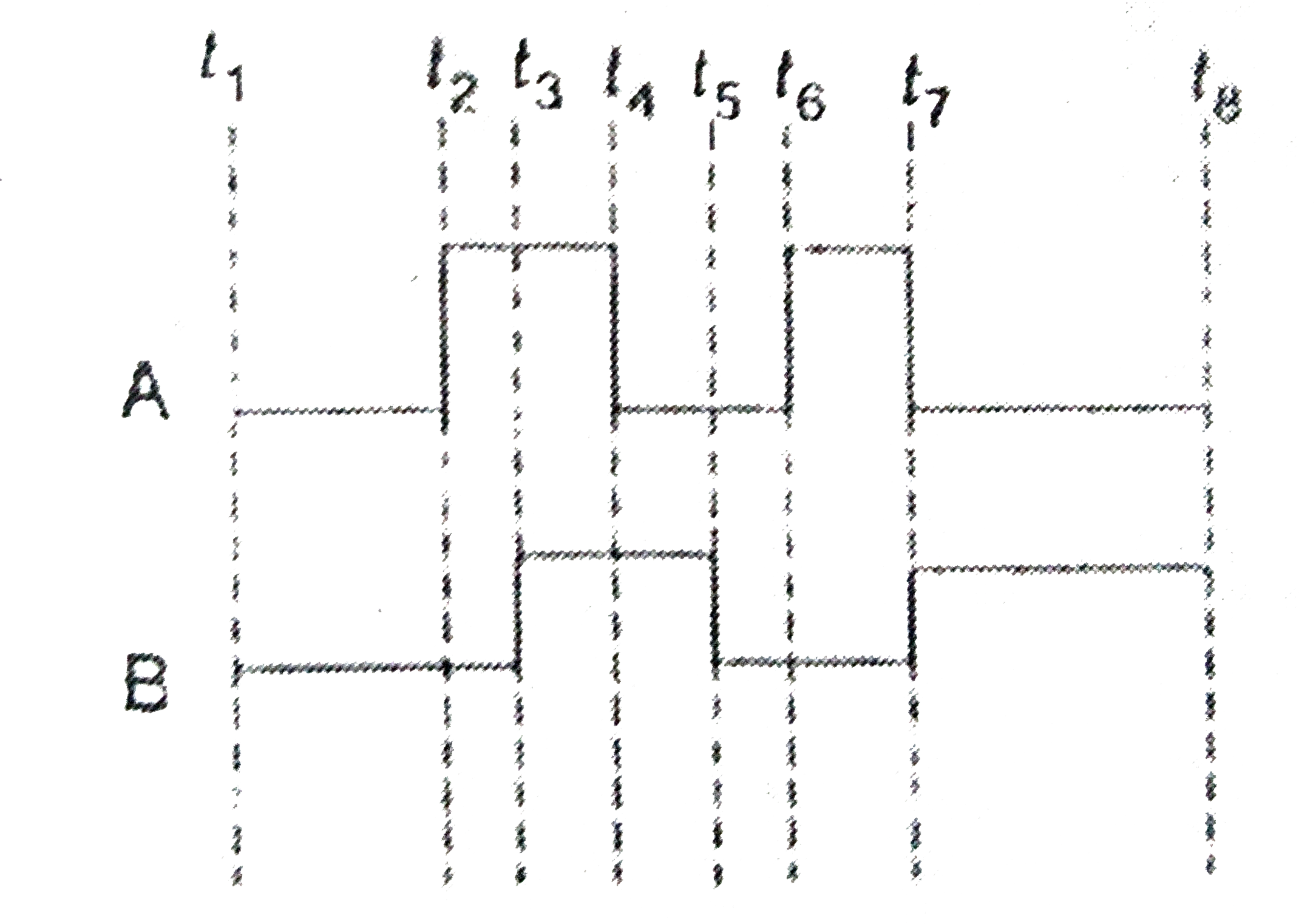
Step by step video & image solution for (a) Draw the circuit diagram of a full wave rectifier using p-n junction diole. Explain its working and show the output, input waveforms. (b) Show the output waveforms (Y) for the following inputs A and B of (i) OR gate (ii) NAND gate : by Physics experts to help you in doubts & scoring excellent marks in Class 12 exams.
Updated on:21/07/2023Similar Questions
Draw the circuit diagram of a half - wave rectifier using a p-n junction diode.
View SolutionShow the output waveform of OR gate for the following input waveforms of A and B

View SolutionShow the output waveform of OR gate for the following input waveforms of A and B
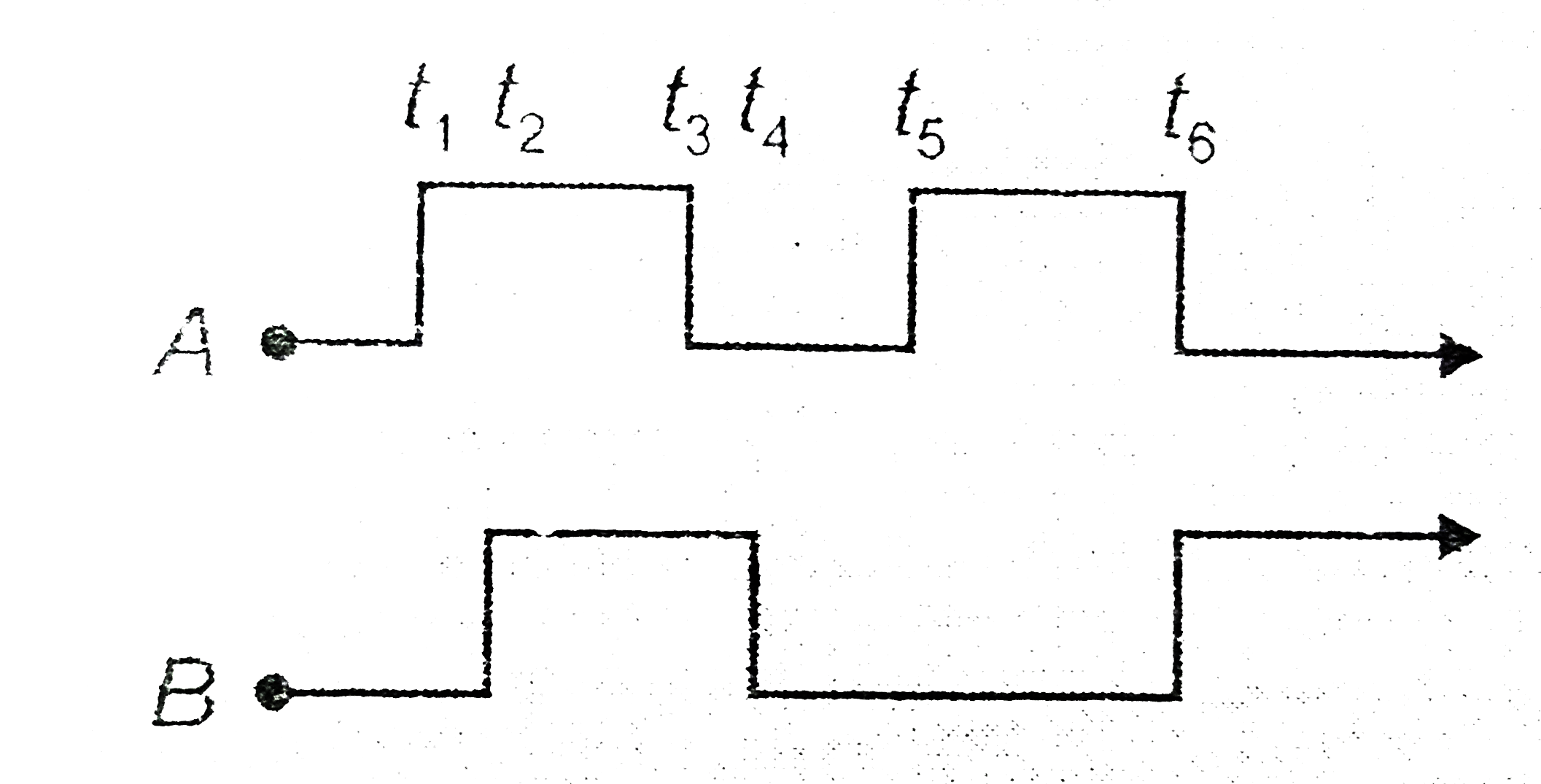
View Solutionshow the output waveform of AND gate for the following input waveforms of A and B.

View SolutionThe output waveform of AND gate for the following input waveforms is
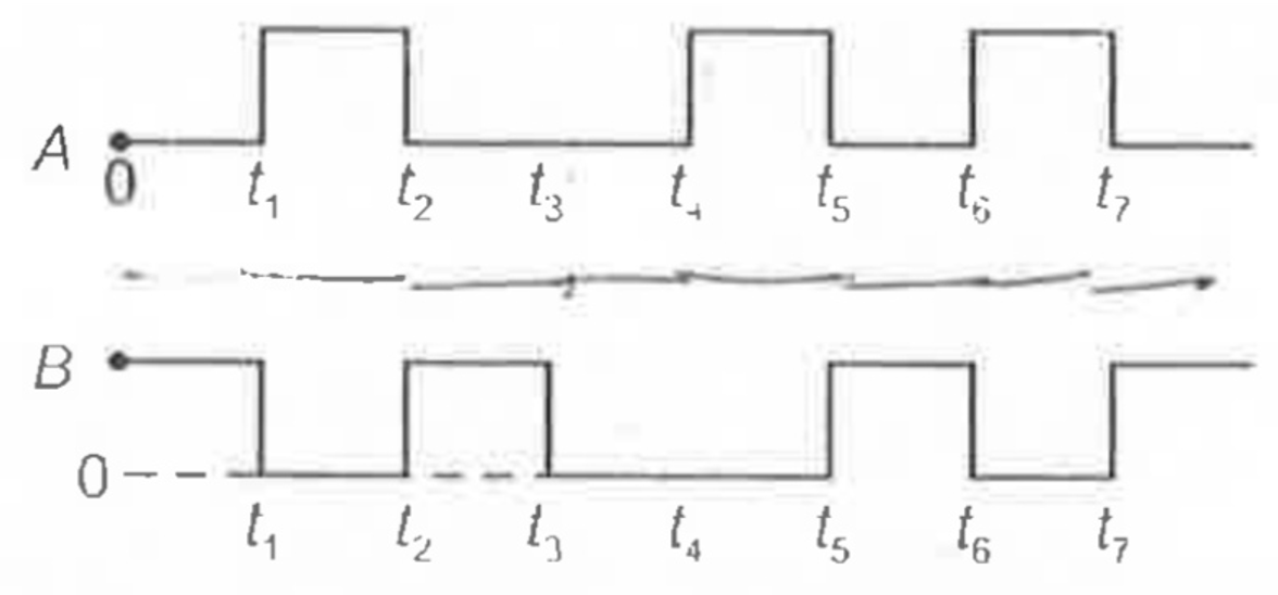
View SolutionSketch the output waveform Y from a NAND gate having following inputs A and B
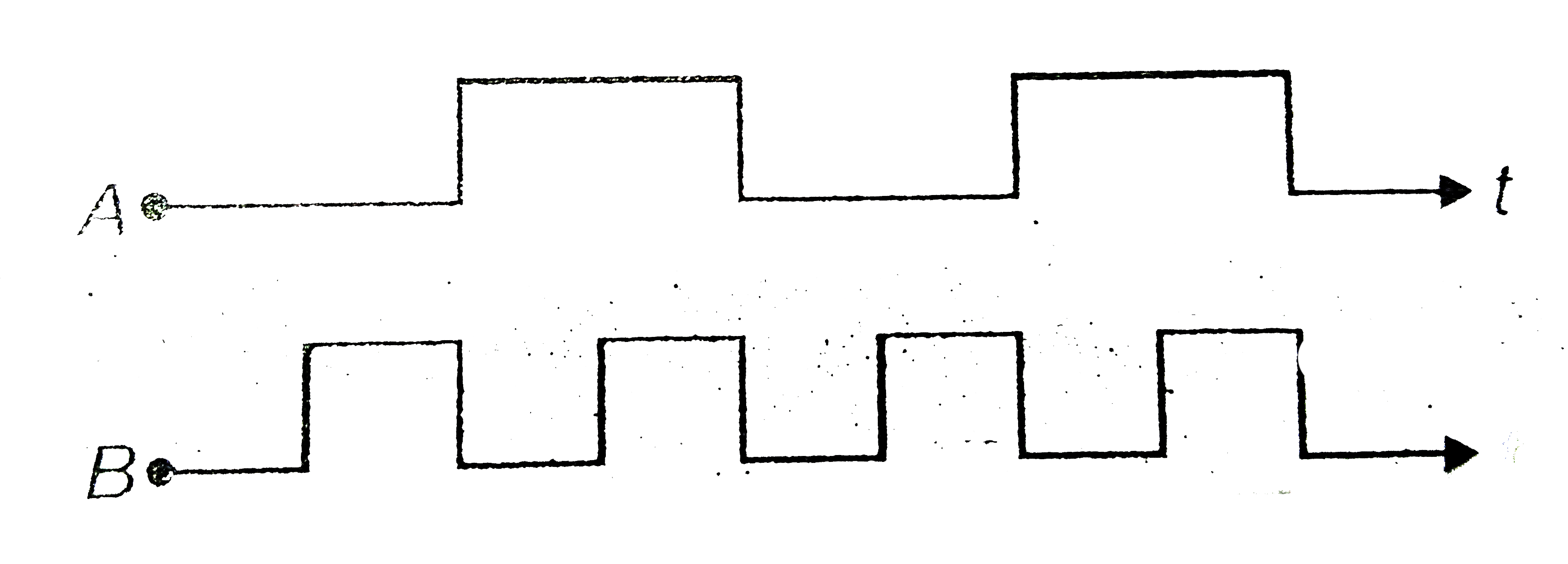
View SolutionSketch the output wavefrom Y from a NAND gate having following inputs A and B
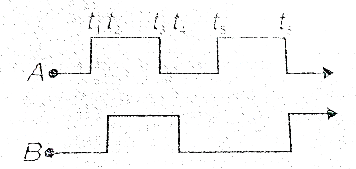
View SolutionDraw the output wave from (Y) of the
(i) OR gate
(ii) NOR gate
(iii) AND gate (iv) NAND gate
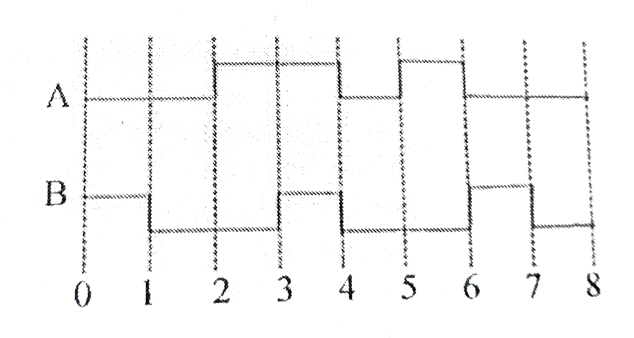
View SolutionSketch the output waveform obtained from AND gate for the following inputs A and B.
View SolutionDraw a labelled circuit diagram of a half wave rectifier and give its output waveform.
View Solution
