Draw the circuit diagram of a half - wave rectifier using a p-n junction diode.
To draw the circuit diagram of a half-wave rectifier using a p-n junction diode, follow these steps:
1. Draw the AC Input Source:
- Begin by drawing a sine wave to represent the alternating current (AC) input. This can be depicted as a pair of horizontal lines with a wavy line between them to indicate the AC waveform.
2. Add a Transformer:
- Next, draw a transformer symbol to step down or step up the voltage as needed. The transformer consists of two coils (primary and secondary) represented by two parallel lines with dots indicating the input and output sides.
3. Insert the P-N Junction Diode:
- Draw the p-n junction diode symbol. The diode symbol consists of a triangle pointing towards a vertical line. The triangle represents the anode (p-type) and the vertical line represents the cathode (n-type). Label the anode and cathode accordingly.
4. Connect the Diode to the Load Resistance:
- After the diode, draw a load resistor (R) connected in series. The resistor can be represented by a zigzag line.
5. Complete the Circuit:
- Finally, connect the load resistor back to the other side of the AC input source to complete the circuit. This will create a closed loop.
6. Label the Components:
- Clearly label the AC source, transformer, diode, and load resistor in your diagram for clarity.
Final Circuit Diagram:
- The final diagram should show the AC input leading to a transformer, which then connects to the p-n junction diode, followed by the load resistor, and returning to the AC source.
- Begin by drawing a sine wave to represent the alternating current (AC) input. This can be depicted as a pair of horizontal lines with a wavy line between them to indicate the AC waveform.
- Next, draw a transformer symbol to step down or step up the voltage as needed. The transformer consists of two coils (primary and secondary) represented by two parallel lines with dots indicating the input and output sides.
- Draw the p-n junction diode symbol. The diode symbol consists of a triangle pointing towards a vertical line. The triangle represents the anode (p-type) and the vertical line represents the cathode (n-type). Label the anode and cathode accordingly.
- After the diode, draw a load resistor (R) connected in series. The resistor can be represented by a zigzag line.
- Finally, connect the load resistor back to the other side of the AC input source to complete the circuit. This will create a closed loop.
- Clearly label the AC source, transformer, diode, and load resistor in your diagram for clarity.
- The final diagram should show the AC input leading to a transformer, which then connects to the p-n junction diode, followed by the load resistor, and returning to the AC source.
Similar Questions
(a) Draw the circuit diagram of a full wave rectifier using p-n junction diole. Explain its working and show the output, input waveforms.
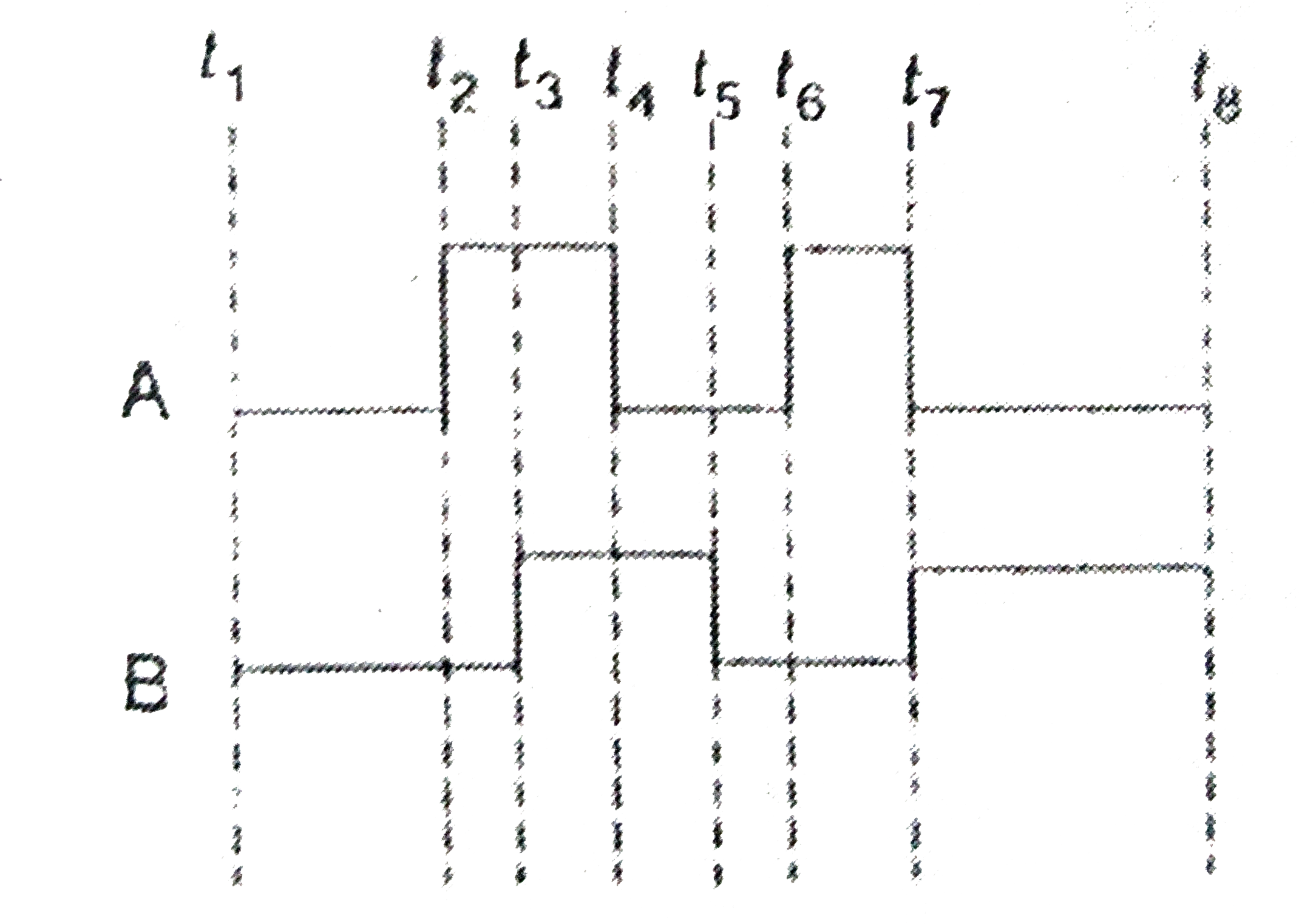
(b) Show the output waveforms (Y) for the following inputs A and B of (i) OR gate (ii) NAND gate :
View SolutionDraw a neatly labelled circuit diagram of a full wave rectifier using two junction diodes.
View Solution
Knowledge Check
Which is the correct diagram of a half- wave reactifier?
A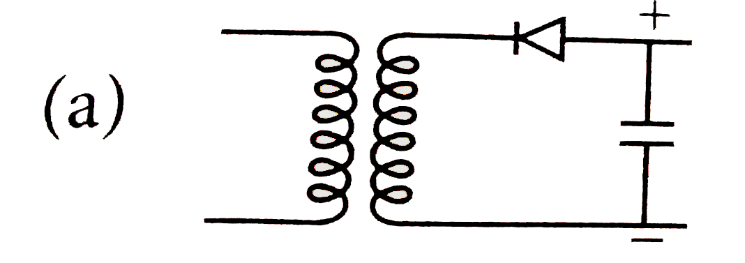 B
B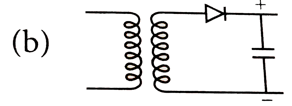 C
C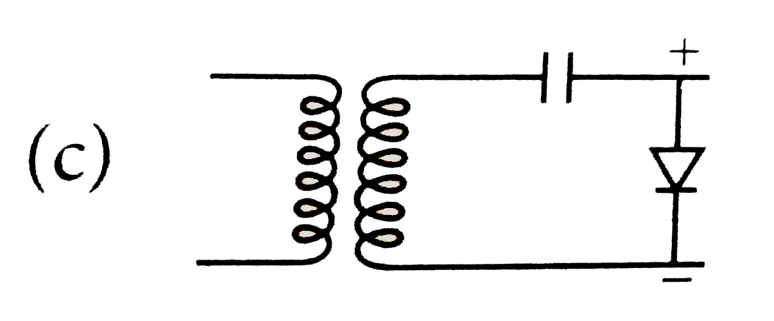 D
D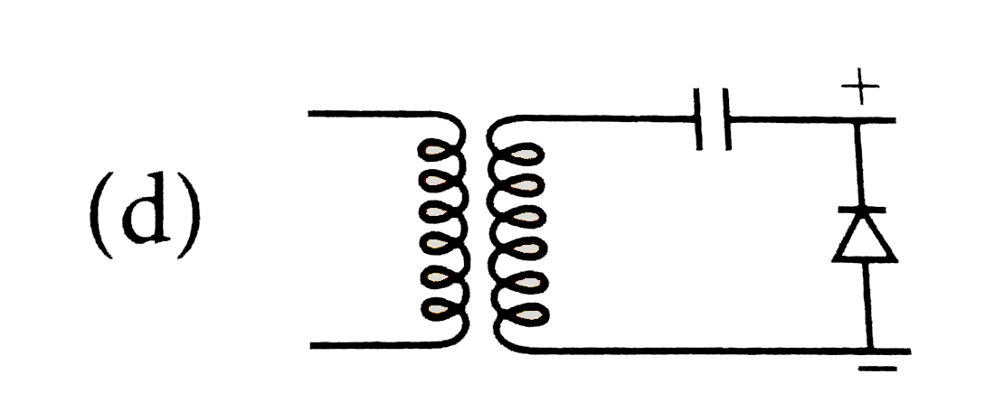
Explain the formation of depletion layer and potential barrier in p-n junction.
Draw the circuit diagram of a half wave rectifier and explain its working.
View SolutionDraw a circuit diagram of a full-wave rectifier. Explain its working principle. Draw the input/output wave forms indicating clearly the function of the two diode used.
View SolutionDraw a circuit diagram of a full-wave rectifier. Explain its working principle. Draw the input/output wave forms indicating clearly the function of the two diode used.
View SolutionDraw a labelled circuit diagram of a half wave rectifier and give its output waveform.
View SolutionExplain with the help of a circuit diagram, the working of a p−n junction diode as a half wave rectifier.
View SolutionThe P-N junction is-
View Solution

(a) Draw the circuit diagram of reversed bias p-n junction.
(b). Draw the output wavefrom across diode in given circuit.
(c). Draw the truth table for the given logic gate.
View Solution
