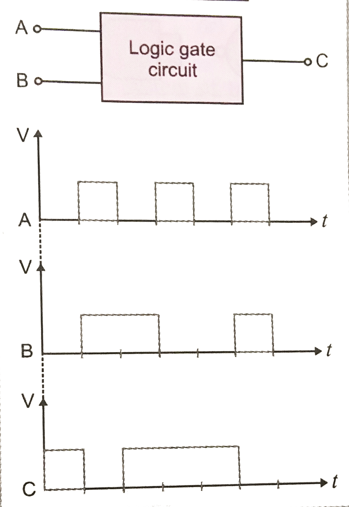
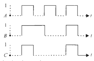
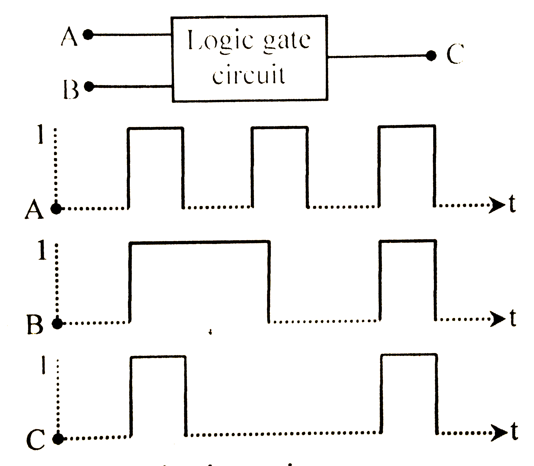
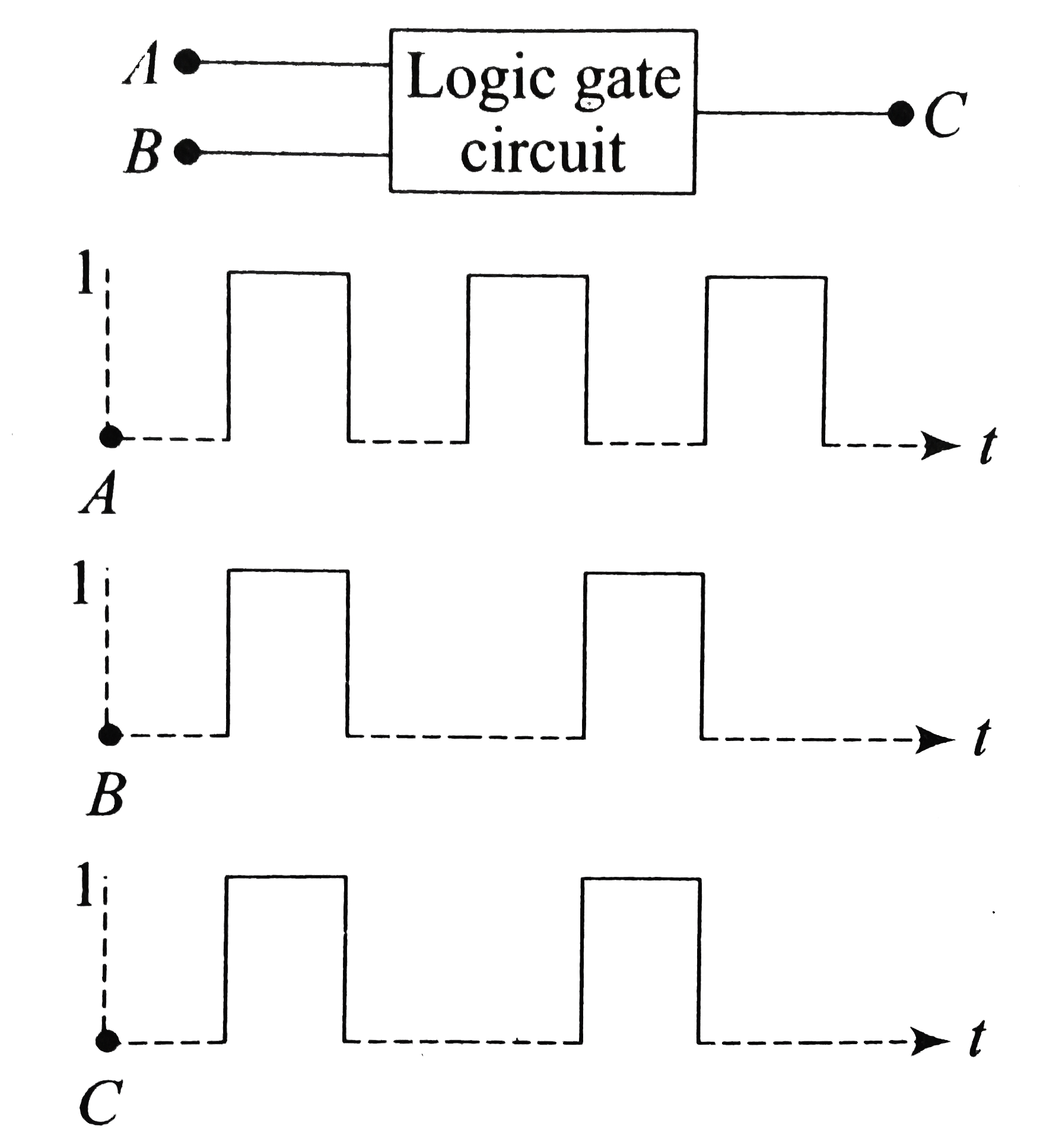
Fig, shows a logic gate circuit with two input A and B and the output C. The voltage wave form of A, B and C are as shown in Fig.The logic gate circuit is
OR gate
AND gate
NOR gate
NAND gate
The correct Answer is:D
Since the output C is at level 0 when both the inputs A and B are of level 1 and output is 1 when both the inputs are 0,0 or 0,1 and 1,0. Hence the logic circuit gate is NAND gate.
Topper's Solved these Questions
- ELECTRONIC DEVICESBook:PRADEEPChapter:ELECTRONIC DEVICESExercise:LONG QUESTION ANSWER
Explore 2 Videos
- ELECTRONIC DEVICESBook:PRADEEPChapter:ELECTRONIC DEVICESExercise:PROBLEMS FOR PRACTICE
Explore 7 Videos
- ELECTRONIC DEVICESBook:PRADEEPChapter:ELECTRONIC DEVICESExercise:HIGHER ORDER THINKING SKILLS
Explore 1 Video
- ELECTROMAGNETIC WAVESBook:PRADEEPChapter:ELECTROMAGNETIC WAVESExercise:II Focus multiple choice question
Explore 5 Videos
- ELECTROSTATICSBook:PRADEEPChapter:ELECTROSTATICSExercise:ASSERTION-REASON TYPE QUESTIONS
Explore 2 Videos
Similar Questions
The following figure shows a logic gate circuit with two inputs A and B and the output C. The voltage waveforms of A, B and C are as shown below.
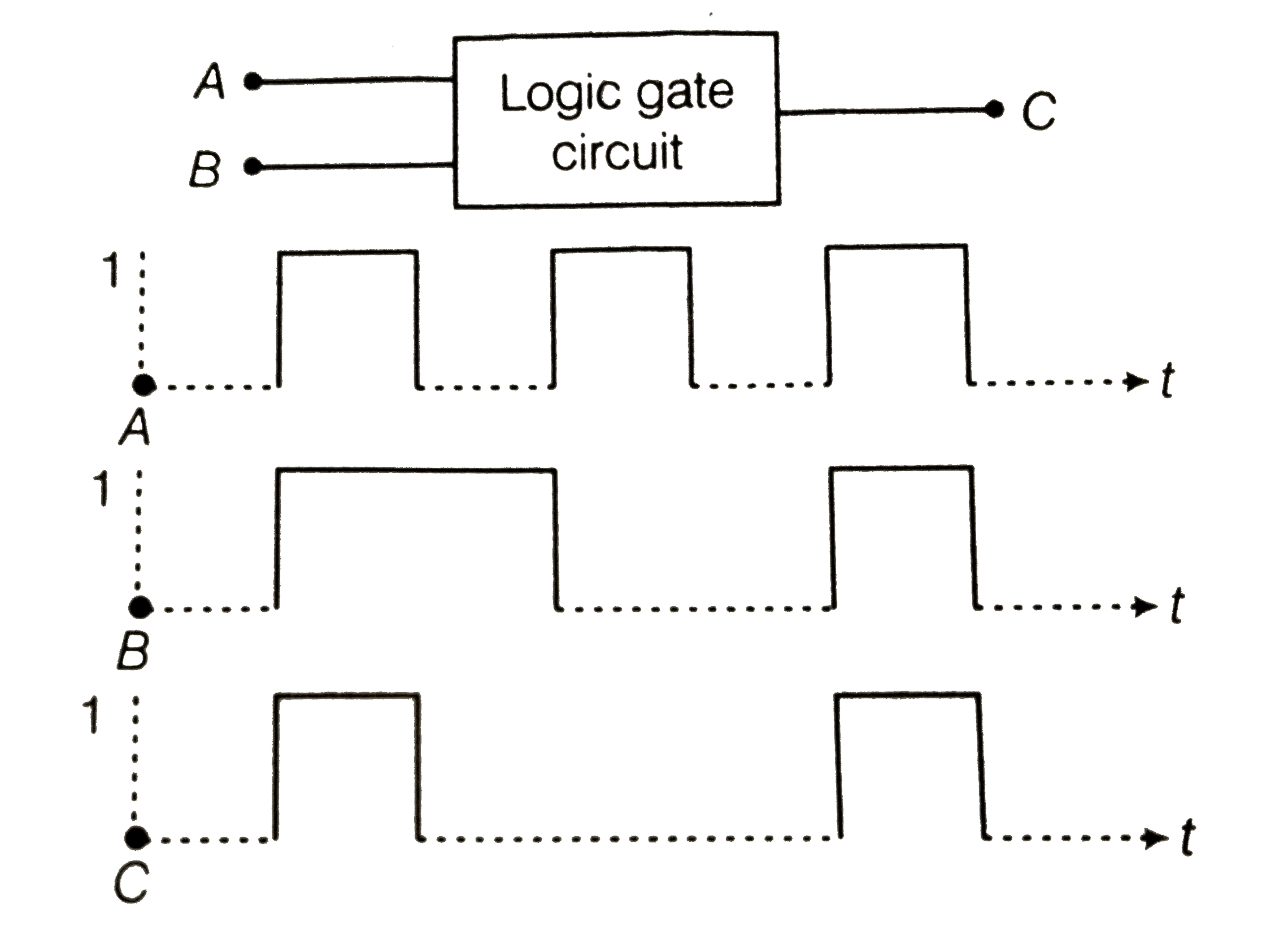
The logic circuit gate is
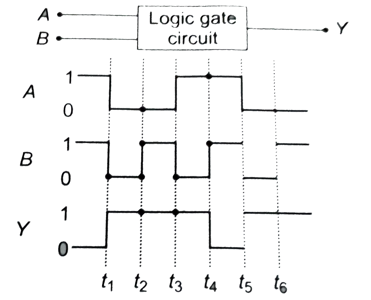
View SolutionThe following figure shows a logic gate circuit with two inputs A and B and the output Y. The voltage waveforms of A,B and the output Y are as given
View Solution
Knowledge Check
The following figure shows a logic gate circuit with two inputs A and B and the output C. The voltage waveforms of A, B and C are as shown below
The logic circuit gate isAAND gateBNAND gateCNOR gateDOR gateThe following figure shows a logic gate circuit with two inputs A and B and the output C. The voltage waveforms of A, B and C are as shown below

The logic circuit gate isAAND gateBNAND gateCNOR gateDOR gateThe following shows a logic gate circuit with two inputs A and B and the output C. The voltage waveforms of A, B and C are as shown below.
The logic circuit gate isAOR gateBAND gateCNAND gateDNOR gate
The following figure shows a logic gate circuit with two inputs A and B and the output Y. The voltage waveforms of A,B and Y are as given :
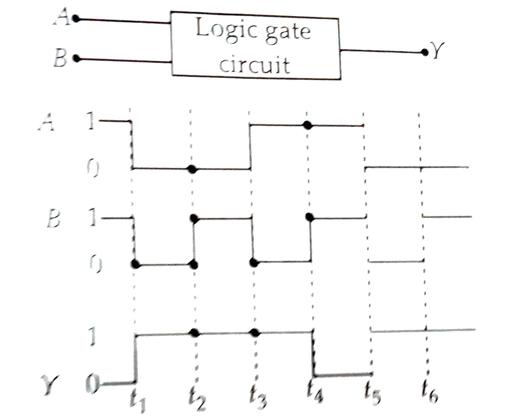
The logic gate is
View SolutionThe figure shows a logic circuit with two inputs A and B and the output C. The voltage wave forms across A,B and C are as given. The logic circuit gate is
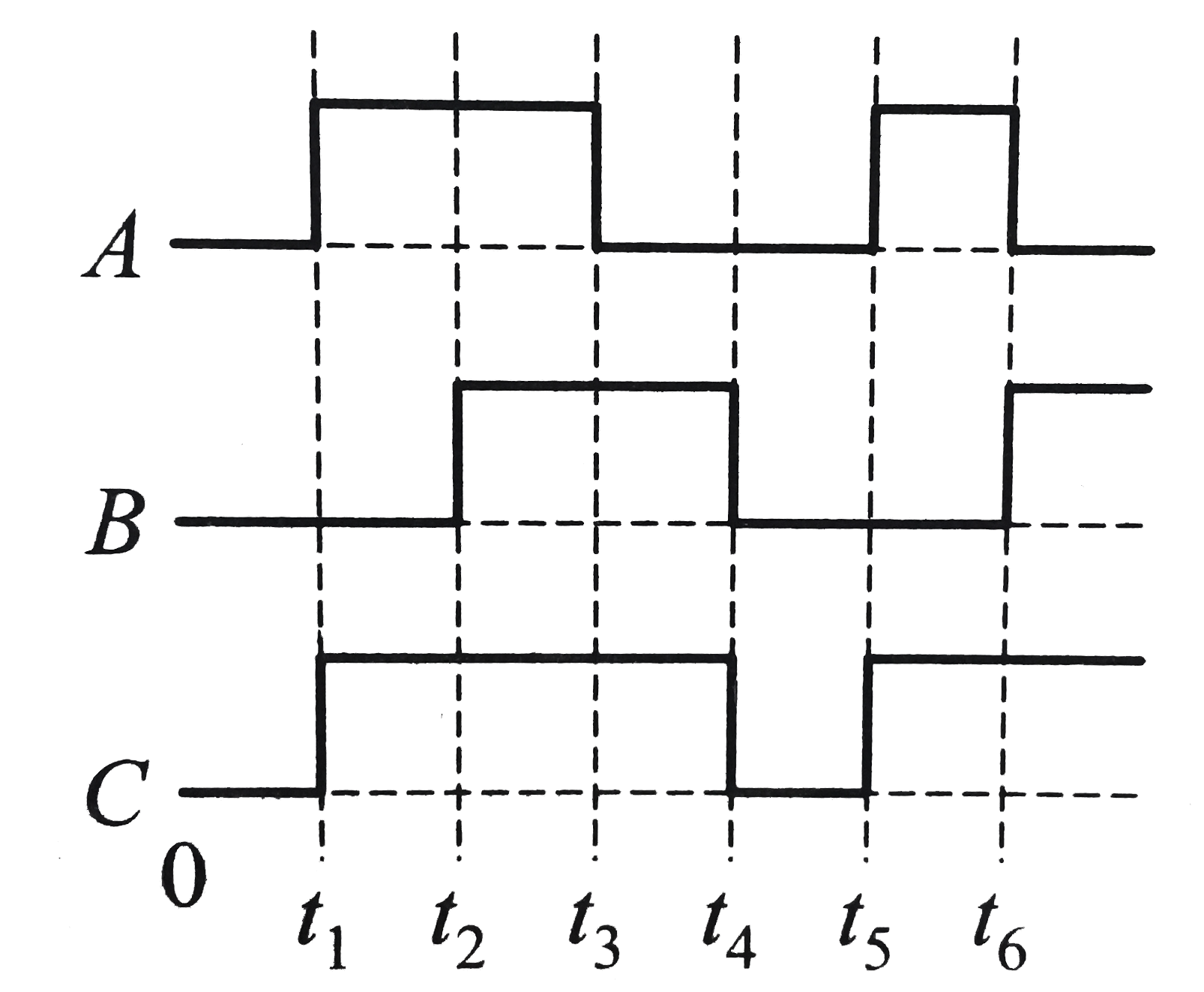
View SolutionThe figure shows a logic circuit with two inputs A and B and the output C. The voltage wave forms across A,B and C are as given. The logic circuit gate is

View SolutionThe following figure shows a logic gate circuit with two inputs A and B and the output C. The voltage waveforms of A, B and C are as shown below-
View SolutionThe following figure shows a logic gate circuit with two inputs A and B and the output C. The voltage waveforms of A,B and C are as shown below
View Solution