Explain the working of p-n junction diode as a full wave rectifier with circuit diagram. Give input and output waveforms.

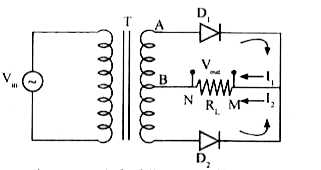
The circuit connections are made for full wave rectifier as shown in circuit diagram. The circuit contains ac source, step down centre tapped transformer(T), two diodes ( and ) and a load resistance .
During positive half cycle of input ac, the point A is possitive with respect to the point B. Then is forward biased and is reverse biased. Thus allows current through the load from M to N.
During negative half cycle of input ac, the point A is negative with respect to the point B. Then is reverse biased and is forward biased. Thus allows current through from A to B.
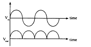
Thus the diodes allows both positive and negative half cycles of input ac through in the same direction (from M to N). Hence the diode acts as full wave rectifier. Input and output wave forms as below

Topper's Solved these Questions
- SUPPLEMENTARY EXAM QUESTION PAPER JULY - 2014Book:SUNSTAR PUBLICATIONChapter:SUPPLEMENTARY EXAM QUESTION PAPER JULY - 2014Exercise:PART-D (VI. Answer any three of the following questions.)
Explore 5 Videos
- SUPPLEMENTARY EXAM QUESTION PAPER JULY - 2014Book:SUNSTAR PUBLICATIONChapter:SUPPLEMENTARY EXAM QUESTION PAPER JULY - 2014Exercise:PART-D (IV. Answer any two of the following questions.)
Explore 3 Videos
- P.U. BOARD LATEST MODEL QUESTION PAPER-3Book:SUNSTAR PUBLICATIONChapter:P.U. BOARD LATEST MODEL QUESTION PAPER-3Exercise:PART-D
Explore 11 Videos
- SUPPLEMENTARY EXAM QUESTION PAPER JULY -2015Book:SUNSTAR PUBLICATIONChapter:SUPPLEMENTARY EXAM QUESTION PAPER JULY -2015Exercise:PART-D
Explore 11 Videos
Similar Questions
What is rectifier explain the working of junction diode as a full wave rectifier diagram
View SolutionDraw a circuit diagram of a full-wave rectifier. Explain its working principle. Draw the input/output wave forms indicating clearly the function of the two diode used.
View SolutionState the principle of working of p-n doide as a rectifier with the help of circuit diagram explain rdraw input and output wave forms
View SolutionWhat is rectifier explain the working of junction diode as a full wave rectifier diagram
View SolutionDraw the circuit diagram of a full wave rectifier. Explain its working showing its input and output waveforms.
View SolutionWhat is a rectifier explain the working of P-N diode as half wave rectifier
View SolutionExplain with the help of a circuit diagram, the working of a p−n junction diode as a half wave rectifier.
View SolutionExplain with the help of a circuit diagram, the working of a p−n junction diode as a half wave rectifier.
View SolutionWith the help of circuit diagram explain, the working of p-n junction diode as half wave rectifier.
View SolutionExplain with the help of a circuit diagram, the working of a p-n junction diode as a half-wave rectifier.
View Solution
