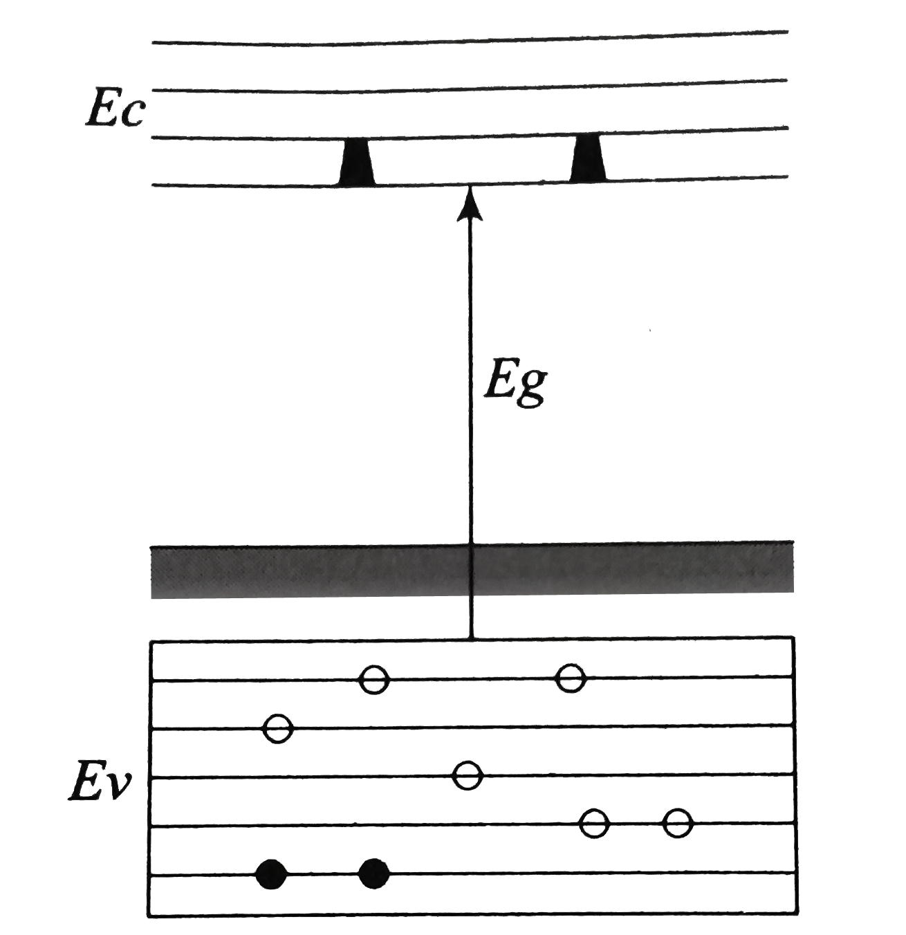
In the energy band diagram of a material shown below, the open circles and filled circles denote holes and electrons respectively. The material is a/an

an n-type semiconductor
a p-type semiconductor
an insulator
a metal
The correct Answer is:B
Step by step video & image solution for In the energy band diagram of a material shown below, the open circles and filled circles denote holes and electrons respectively. The material is a/an by Physics experts to help you in doubts & scoring excellent marks in Class 12 exams.
Updated on:21/07/2023Similar Questions
Which of the energy band diagrams shown in the figure corresponds to that of a semiconductor?
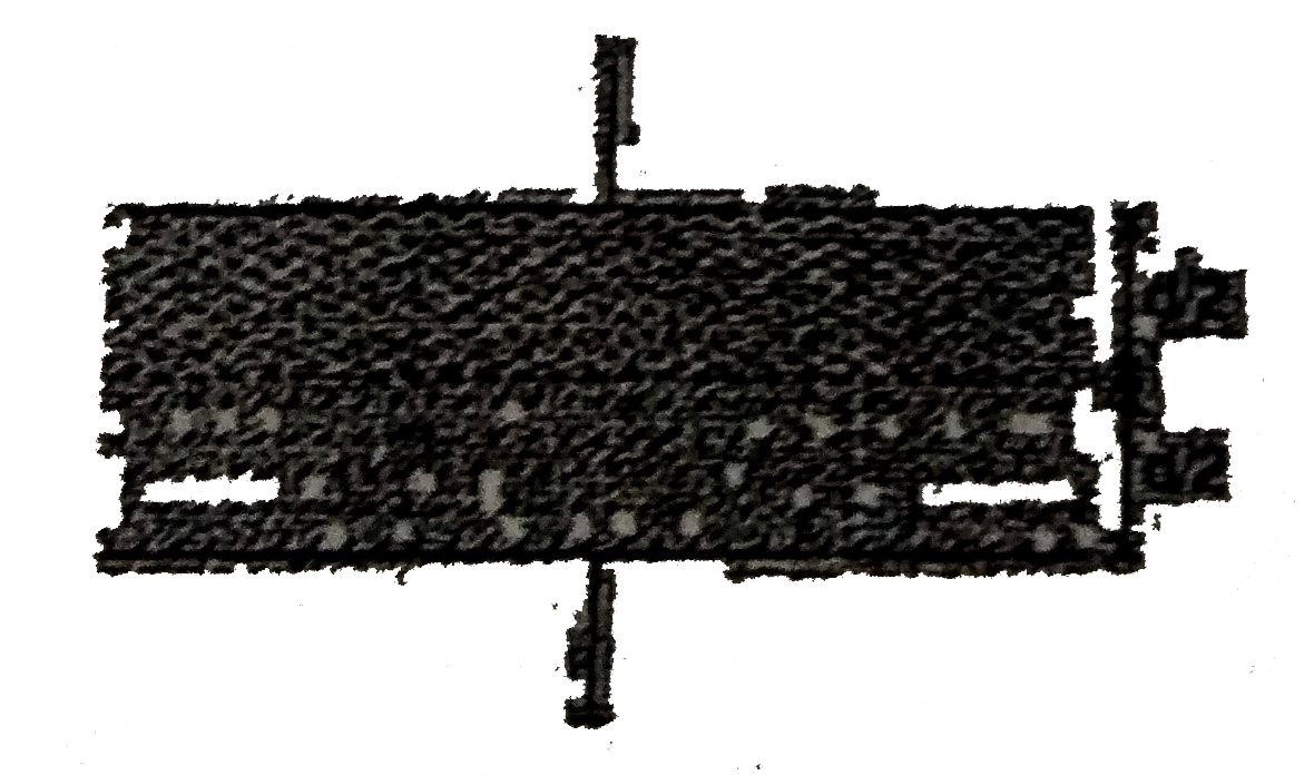
View SolutionA parallel plate capacitor of plate area A and separation d is filled with two materials each of thickness d2 and dielectric constants ∈1 and ∈2 respectively. The equivalent capacitance will be

View Solution
Knowledge Check
Assertion: If there is some gap between the conduction band and the valence band, electrons in the valence band all remain bound and no free electrons are available in the conduction band. Then the material is an insulator.
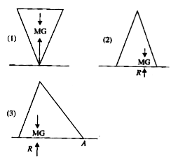
Reason: Resistance of insulators is very lowAIf both assertion and reason are true and reason is the correct explanation of assertion.BIf both assertion and reason are true not but reason is not the correct explanation of assertion.CIf assertion is true but reason is falseDIf both assertion and reason are false.The system shown in the figure diagrams labelled (1), (2) and (3) below represent respectively
 Aneutral, stable and unstable equilibriaBstable, unstable and neutral equilibriaCunstable, stable and neutral equilibriaDneutral, unstable and stable equilibria
If p is the resistivity of a material, and n is the number density of free electrons in it, the mean time between collisions between electrons in the material is given by: (m denotes the mass of an electron, and e denotes the charge on an electron)
View SolutionDraw the Energy bands 'diagrams for a (i) pure semiconductor , (ii) insulator , How does the energy band, for a pure semiconductor , get affected when this semiconductor is doped with (a) an acceptor impurity
(b) donor impurity ? Hence discuss why the 'holes' and the 'electrons' respectively, become the 'majority change carries' in these two cases ?
Write the two processes involved in the formation of p−n junction.

View SolutionIn a semiconducting material the mobilities of electrons and holes are μe and μh respectively. Which of the following is true?
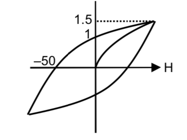
View SolutionThe hysteresis curve for a material is shown in the figure. Then for the material retentivity, coercivity and saturation magnetization respectively will be
View SolutionThe hysteresis curve for a material is shown in the figure. Then for the material retentivity, coercivity and saturation magnetization respectively will be

View SolutionThe energy of a photon of sodium light (λ=589nm)equal the band gap of a semiconducting material.(a)Find the minimum energy E requried to create a hole-electron pair.(b)Find the value of E/kTat a temperature of 300K.
View Solution
