In a p-n junction having depletion layer of thickness m the potential across it is . Then the electric field is
Hint =
The correct Answer is:B
To find the electric field (E) across a p-n junction with a given depletion layer thickness (d) and potential (V), we can use the formula:
E=Vd
1. Identify the given values:
- Thickness of the depletion layer, d=10−6 m
- Potential across the depletion layer, V=0.3 V
2. Substitute the values into the formula:
E=Vd=0.3V10−6m
3. Calculate the electric field:
E=0.310−6=0.3×10⁶V/m
E=3×10⁵V/m
4. Final Result:
The electric field across the depletion layer is E=3×10⁵V/m.
Conclusion:
The correct option for the electric field is option 2: 3×10⁵V/m.
- Thickness of the depletion layer, d=10−6 m
- Potential across the depletion layer, V=0.3 V
E=Vd=0.3V10−6m
E=0.310−6=0.3×10⁶V/m
E=3×10⁵V/m
The electric field across the depletion layer is E=3×10⁵V/m.
The correct option for the electric field is option 2: 3×10⁵V/m.
Topper's Solved these Questions
- SEMICONDUCTOR ELECTRONICS (MATERIAL, DEVICES AND SIMPLE CIRUITS )BOOK - AAKASH INSTITUTE ENGLISHCHAPTER - SEMICONDUCTOR ELECTRONICS (MATERIAL, DEVICES AND SIMPLE CIRUITS )EXERCISE - EXERCISE
20 Videos
- SEMICONDUCTOR ELECTRONICS (MATERIAL, DEVICES AND SIMPLE CIRUITS )BOOK - AAKASH INSTITUTE ENGLISHCHAPTER - SEMICONDUCTOR ELECTRONICS (MATERIAL, DEVICES AND SIMPLE CIRUITS )EXERCISE - Assignment section -A (Objective Type Question)
43 Videos
- SEMICONDUCTOR ELECTRONICS (MATERIAL, DEVICES AND SIMPLE CIRUITS )BOOK - AAKASH INSTITUTE ENGLISHCHAPTER - SEMICONDUCTOR ELECTRONICS (MATERIAL, DEVICES AND SIMPLE CIRUITS )EXERCISE - Assignment SECTION - D (Assertion & reason type Question)
10 Videos
- RAY OPTICS AND OPTICAL INSTRUMENTSBOOK - AAKASH INSTITUTE ENGLISHCHAPTER - RAY OPTICS AND OPTICAL INSTRUMENTSEXERCISE - ASSIGNMENT (SECTION - D)
16 Videos
- SEMICONDUCTOR ELECTRONICS: MATERIALS, DEVICES AND SIMPLE CIRCUITSBOOK - AAKASH INSTITUTE ENGLISHCHAPTER - SEMICONDUCTOR ELECTRONICS: MATERIALS, DEVICES AND SIMPLE CIRCUITSEXERCISE - Assignment (Section-D (Assertion and reason))
5 Videos
Similar Questions
Knowledge Check
A potential barrier of 0.50V exists across a P−N junction. If the depletion region is 5.0×10⁻⁷m, wide the intensity of the electric field in this region is
A106 V/mB107 V/mC105 V/mD104 V/mA potential barrier of 0.3 V exists across a p-n junction. If the depletion region is 1 μm wide, what is the intensity of electric field in this region?
A2×105Vm−1B3×105Vm−1C4×105Vm−1D5×105Vm−1
In a p−n junction diode having depletion layer of thickness 10−6m, the potential across it is 1V. The electric field produced is
View SolutionThe depletion layer in diode is 1μm wide and the knee potential is 0.6V, then the electric field in the depletion layer will be
View SolutionIn a p-n junction, the thickness of depletion region is 2×10⁻⁷m and potential barrier across the junction is 0.20 V
What will be the intensity of electric field in this region ?
View SolutionA potential barrier of 0.50V exists across a p-n junction.(a) If the depletion region is 5.0×10⁻⁷m wide,what is the intensity of the electric field in this region?(b) An electron with speed5.0×105ms−1approaches the p-n junction form the n-side.With what speed will it enter the p-side?
View SolutionFind the potential V at P in the gravitational field of fixed point mass M.
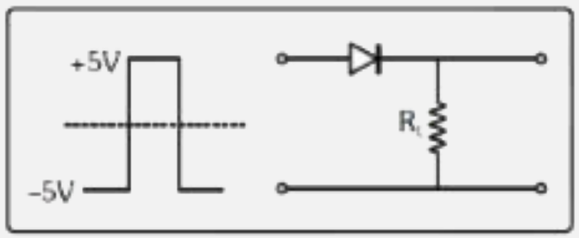
View SolutionIf in a p-n junction, a square input signal of 10 V is applied as shwon, then the output across RL will be

View Solution
