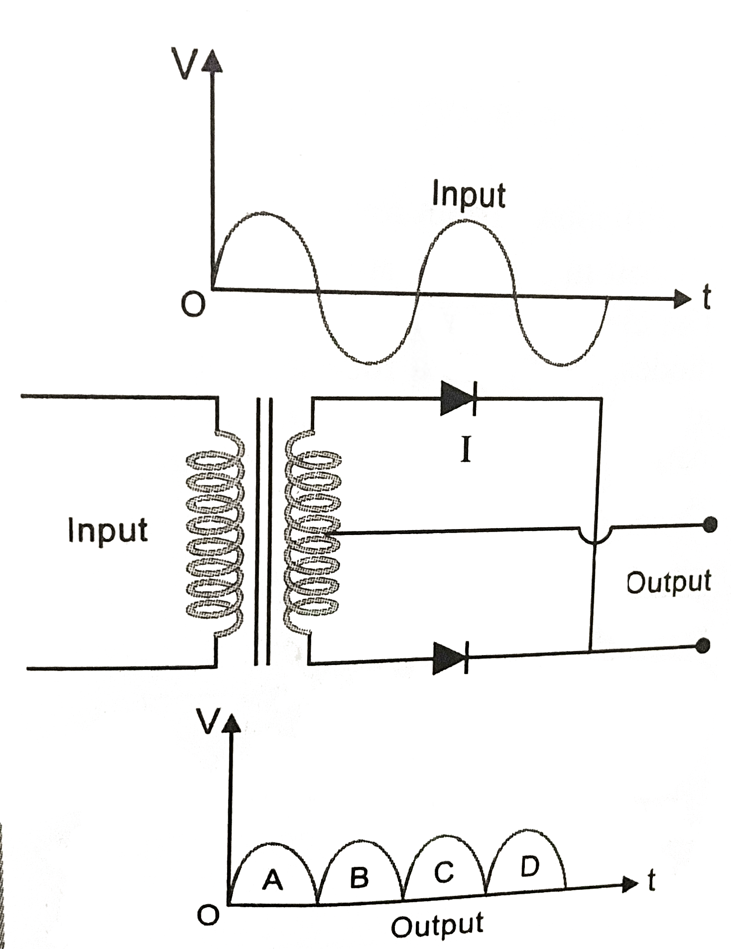
A full wave rectifier circuit along with the input and output are shown in the figure. The contribution from the diode D2 is (are)
C
A, C
B,D
A,B,C,D
The correct Answer is:C
To analyze the contribution from the diode D2 in a full wave rectifier circuit, we can follow these steps:
Step 1: Understand the Full Wave Rectifier Circuit
A full wave rectifier circuit uses two diodes (D1 and D2) to convert an alternating current (AC) input into a direct current (DC) output. The circuit allows both halves of the AC waveform to contribute to the output.
Hint: Remember that in a full wave rectifier, both diodes conduct during different halves of the AC cycle.
Step 2: Analyze the Input Waveform
The input to the full wave rectifier is a sinusoidal AC waveform. This waveform has both positive and negative halves. The positive half will allow diode D1 to conduct, while the negative half will allow diode D2 to conduct.
Hint: Identify which diode conducts during each half of the AC cycle.
Step 3: Determine the Output Waveform
The output waveform of a full wave rectifier will consist of peaks corresponding to the conduction of each diode. During the positive half, D1 conducts and produces output peaks, while during the negative half, D2 conducts and produces its own output peaks.
Hint: Look for the peaks in the output waveform that correspond to the conduction of D2.
Step 4: Identify Contributions from Diode D2
From the output waveform, we can identify the peaks that are associated with diode D2. In the output waveform, the peaks that occur during the negative half of the AC cycle are due to D2. Specifically, these are the second and fourth peaks of the output waveform.
Hint: Focus on the peaks that occur when the input waveform is in its negative half.
Step 5: Conclusion
The contribution from diode D2 can be summarized as the output peaks that occur when D2 is conducting. In the context of the provided question, the peaks labeled B and D in the output waveform are the contributions from diode D2.
Hint: Make sure to clearly label the peaks in your analysis to avoid confusion.
Final Answer
The contribution from the diode D2 is represented by the output peaks B and D.
A full wave rectifier circuit uses two diodes (D1 and D2) to convert an alternating current (AC) input into a direct current (DC) output. The circuit allows both halves of the AC waveform to contribute to the output.
The input to the full wave rectifier is a sinusoidal AC waveform. This waveform has both positive and negative halves. The positive half will allow diode D1 to conduct, while the negative half will allow diode D2 to conduct.
The output waveform of a full wave rectifier will consist of peaks corresponding to the conduction of each diode. During the positive half, D1 conducts and produces output peaks, while during the negative half, D2 conducts and produces its own output peaks.
From the output waveform, we can identify the peaks that are associated with diode D2. In the output waveform, the peaks that occur during the negative half of the AC cycle are due to D2. Specifically, these are the second and fourth peaks of the output waveform.
The contribution from diode D2 can be summarized as the output peaks that occur when D2 is conducting. In the context of the provided question, the peaks labeled B and D in the output waveform are the contributions from diode D2.
The contribution from the diode D2 is represented by the output peaks B and D.
Topper's Solved these Questions
- SEMICONDUCTOR ELECTRONICS (MATERIAL, DEVICES AND SIMPLE CIRUITS )BOOK - AAKASH INSTITUTE ENGLISHCHAPTER - SEMICONDUCTOR ELECTRONICS (MATERIAL, DEVICES AND SIMPLE CIRUITS )EXERCISE - Assignment section -A (Objective Type Question)
43 Videos
- SEMICONDUCTOR ELECTRONICS (MATERIAL, DEVICES AND SIMPLE CIRUITS )BOOK - AAKASH INSTITUTE ENGLISHCHAPTER - SEMICONDUCTOR ELECTRONICS (MATERIAL, DEVICES AND SIMPLE CIRUITS )EXERCISE - Assignment section -B (Objective Type Question)
29 Videos
- SEMICONDUCTOR ELECTRONICS (MATERIAL, DEVICES AND SIMPLE CIRUITS )BOOK - AAKASH INSTITUTE ENGLISHCHAPTER - SEMICONDUCTOR ELECTRONICS (MATERIAL, DEVICES AND SIMPLE CIRUITS )EXERCISE - TRY YOUR SELF
27 Videos
- RAY OPTICS AND OPTICAL INSTRUMENTSBOOK - AAKASH INSTITUTE ENGLISHCHAPTER - RAY OPTICS AND OPTICAL INSTRUMENTSEXERCISE - ASSIGNMENT (SECTION - D)
16 Videos
- SEMICONDUCTOR ELECTRONICS: MATERIALS, DEVICES AND SIMPLE CIRCUITSBOOK - AAKASH INSTITUTE ENGLISHCHAPTER - SEMICONDUCTOR ELECTRONICS: MATERIALS, DEVICES AND SIMPLE CIRCUITSEXERCISE - Assignment (Section-D (Assertion and reason))
5 Videos
Similar Questions
Knowledge Check
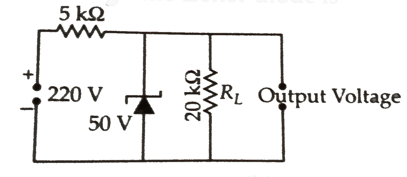
From the Zener diode circuit shown in figure, the current through the Zener diode is
 A34 mAB31.5 mAC36.5 mAD2.5 mA
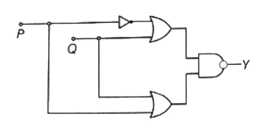
To get an output 1 from the circuit shown in figure the input must be :

View SolutionIn the given circuit P and Q from the inputs. The output Y is

View SolutionTo get an output of 1 form the circuit shown in figure the input must be :-
_E01_514_Q01.png)
View SolutionDraw a circuit diagram of a full-wave rectifier. Explain its working principle. Draw the input/output wave forms indicating clearly the function of the two diode used.
View SolutionDraw a circuit diagram of a full-wave rectifier. Explain its working principle. Draw the input/output wave forms indicating clearly the function of the two diode used.
View SolutionIn the circuit shown in the figure, in steady state:
The current drawn from the battery is
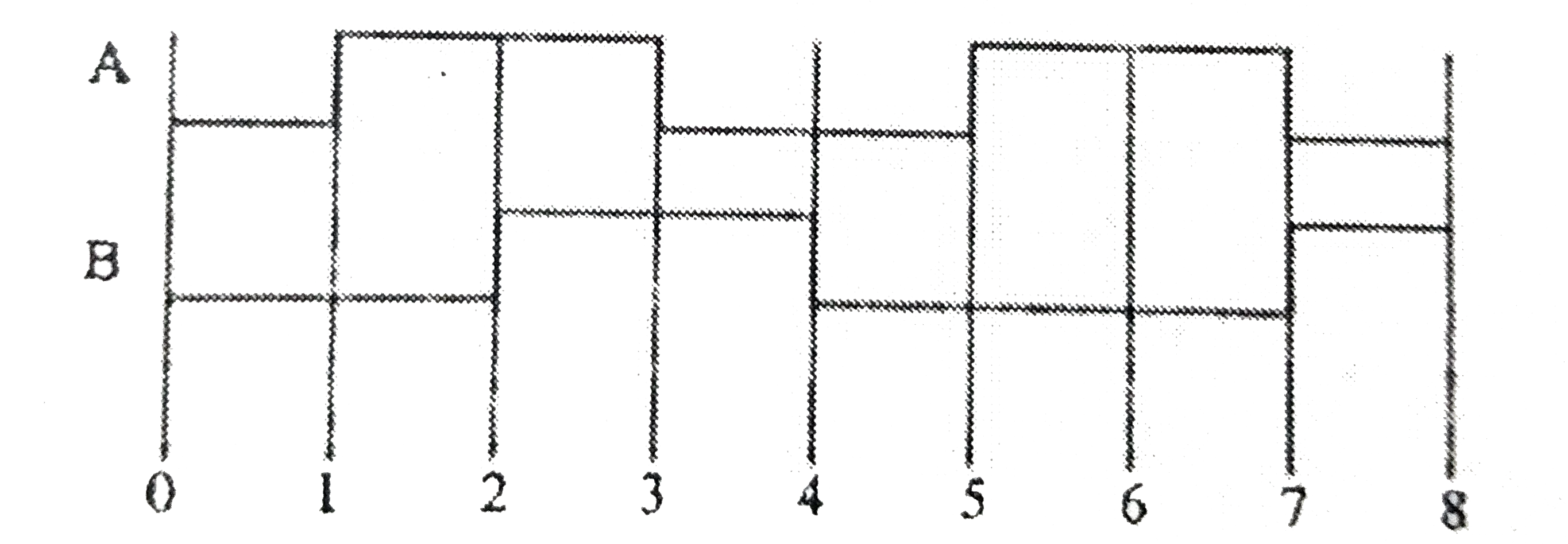
View Solution(i) Sketch the output waveform from an AND gate for the inputs A and B shown in the figure.

(ii) If the output of the above AND gate is fed to a NOT gate, name the gate of the combination so formed.
View Solution


