The cause of the potential barrier in a p-n diode is
Depletion of negative charges near the junction
Concentration of positive charges near the junction
Depletion of positive charges near the junction
Concentration of positive and negative charges near the junction
The correct Answer is:D
Step by step video & image solution for The cause of the potential barrier in a p-n diode is by Physics experts to help you in doubts & scoring excellent marks in Class 12 exams.
Updated on:21/07/2023Topper's Solved these Questions
- SEMICONDUCTOR ELECTRONICS (MATERIAL, DEVICES AND SIMPLE CIRUITS )BOOK - AAKASH INSTITUTE ENGLISHCHAPTER - SEMICONDUCTOR ELECTRONICS (MATERIAL, DEVICES AND SIMPLE CIRUITS )EXERCISE - Assignment SECTION - D (Assertion & reason type Question)
10 Videos
- SEMICONDUCTOR ELECTRONICS (MATERIAL, DEVICES AND SIMPLE CIRUITS )BOOK - AAKASH INSTITUTE ENGLISHCHAPTER - SEMICONDUCTOR ELECTRONICS (MATERIAL, DEVICES AND SIMPLE CIRUITS )EXERCISE - Assignment section -B (Objective Type Question)
29 Videos
- RAY OPTICS AND OPTICAL INSTRUMENTSBOOK - AAKASH INSTITUTE ENGLISHCHAPTER - RAY OPTICS AND OPTICAL INSTRUMENTSEXERCISE - ASSIGNMENT (SECTION - D)
16 Videos
- SEMICONDUCTOR ELECTRONICS: MATERIALS, DEVICES AND SIMPLE CIRCUITSBOOK - AAKASH INSTITUTE ENGLISHCHAPTER - SEMICONDUCTOR ELECTRONICS: MATERIALS, DEVICES AND SIMPLE CIRCUITSEXERCISE - Assignment (Section-D (Assertion and reason))
5 Videos
Similar Questions
Knowledge Check
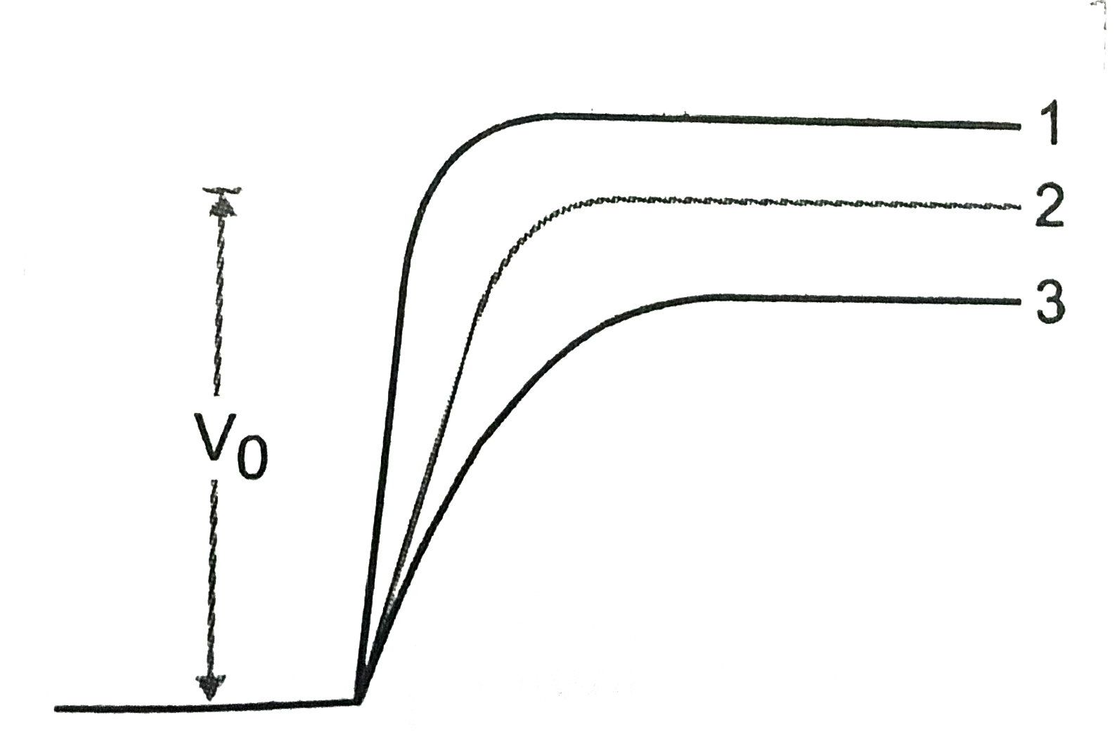
In Fig . V0 is the potential barrier across a p-n junction, when no battery is connected across the junction
 A1 and 3 both correspond to forward bias of junctionB3 corresponds to forward bias of junction and 1 corresponds to reverse bias of junctionC1 corresponds to forward bias and 3 corresponds to reverse bias of junction.D3 and 1 both correspond to reverse bias of junction.
In a forward biased PN- junction diode, the potential barrier in the depletion region is of the from...
View SolutionConsider the following statements A and B and identify the correct answer
(A) A Zener diode is always connected in reverse bias to use it as voltage regulator.
(B) The potential barrier of a p−n junction lies between 0.1 to 0.3V, approximately.
View SolutionIn a forward biased p - n junction diode , which of the following graphs is most appropriately represented the potential barrier in the depletion .region ?
View SolutionCan the potential barrier across a p−n junction be measured by simply connecting a voltmeter across the junction ?
View SolutionIn Fig . V0 is the potential barrier across a p-n junction, when no battery is connected across the junction

View SolutionCan the potential barrier across a p-n junction be measured by simply connecting a voltmeter across the junction ?
View SolutionThe increase in the width of the depletion region in a p-n junction diode is due to:
View Solution

